The Shift Register, Bus and Reset logic

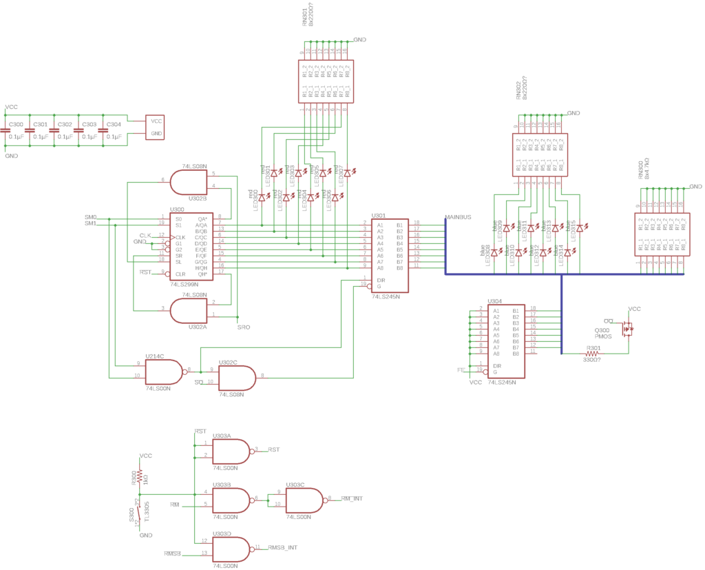
This page contains a few small independent modules. The largest one is the shift register, which occupies most of the left half of the page. A shift register can be used just like any other register, but it has an additional ability: it can shift the binary value inside it to the left or right. This can be quite useful in programming and calculations, as a shift to the left corresponds to a multiplication by 2 (and a right shift is a division by 2). I simply used a dedicated 8-bit shift register chip (74LS299, U300 on the left) to implement this.
Usually, when shifting, the outermost bit that gets “shifted out” is simply discarded and the other side of the byte is filled with a zero. But sometimes, it can be useful to keep that bit and push it back into the other side of the byte instead. That operation is called a “roll”, and it is implemented using the two AND gates next to the chip. That way, the program can use the SRO (shift roll-over) control signal to enable this feature. In addition to the register chip, it also features a bus transceiver and LEDs as before, except that the bus transceiver is used bidirectionally here, both for reading and writing data to/from the shift register.
The next part of this page, on the right side, contains some utilities for the main bus. There is an LED pack to show what is currently on the bus, as well as some pull-down resistors to hold the bus at all zeroes when no module is outputting data to it. Then there’s a bus transceiver and a transistor, which the control logic can use to set the bus to the values 01, FE or FF (hexadecimal) instead of the default 00. That is useful for the quick implementation of some instructions.
Finally, this page houses the logic for the main reset signals of the computer (bottom left). The reset is triggered by the button S300. From that, the circuit produces reset signals in both polarities (active high and active low) that are distributed to all memory-containing modules, resetting the computer’s state (but not clearing the RAM). It also handles the two smaller reset signals RM and RMSB, which can be triggered either by the main reset or by the control logic.
The RAM and Z register

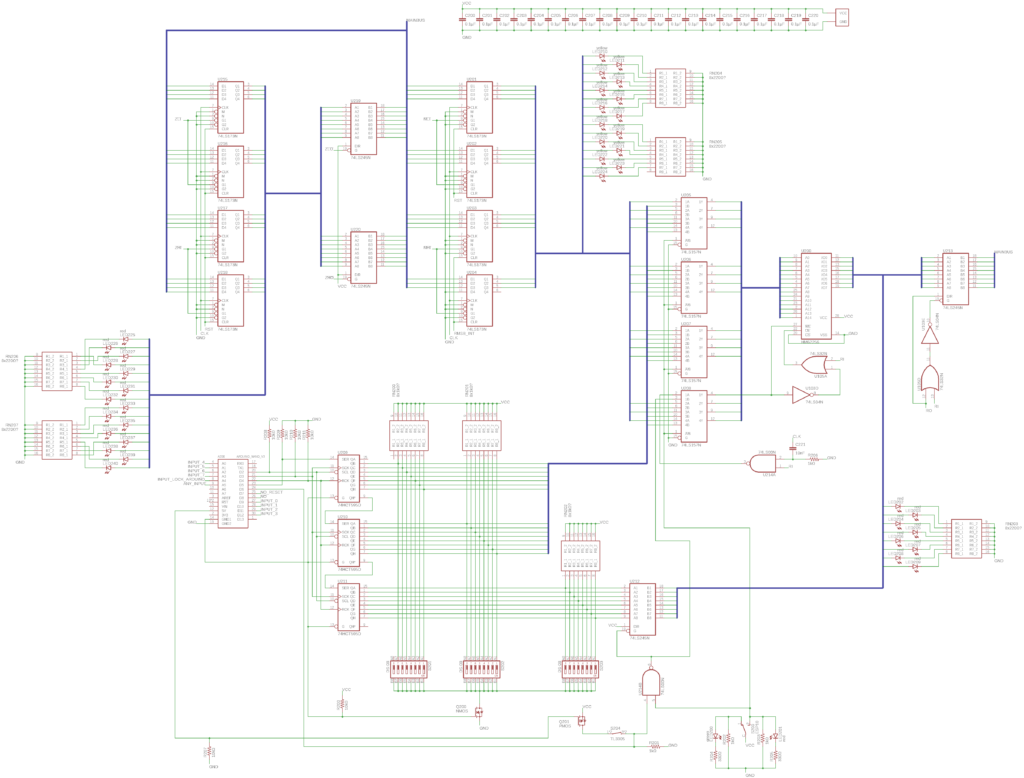
Now, we get to the largest page of the schematic. It contains the RAM (Random Access Memory), the memory address register, programming logic, and the general-purpose 16-bit register Z. The RAM module is relatively similar to Ben’s design, but expanded by a lot – from 16 bytes to 32KB.
The RAM chip itself (HM62256) is the largest schematic symbol on the page (U200 in the middle right area). On its right side is the memory data bus which is used to transfer data (one byte at a time) to and from the memory. It’s connected to the main bus through a bus transceiver (directly to the right of the RAM chip). On the left side is the 15-bit-wide memory address bus, giving it a total of 32768 memory locations (=32KB of memory).
The RAM module is relatively complex because there are two separate ways that the RAM needs to be accessed: by the computer, when running a program, and by the user/Arduino, when programming the computer (writing the program into memory). Both of these supply an address and data. Therefore, the module must select one of the given addresses (program address or externally supplied address) and the corresponding data lines, based on whether the computer is running or being programmed. This also happens in Ben’s design.
The user must select between “run” mode and “programming” mode using the switch S200, which you can see at the bottom right of the page. Based on that signal, the address is selected, using 4 selector chips (74LS157) that you can see on the left of the main RAM chip.
The address for “run” mode is stored in the 15-bit memory address register (top middle) which is made of four 4-bit register chips. The data in “run” mode is provided by the main bus, through the bus transceiver mentioned above.
In “programming” mode, the address and data are provided either by manual switches (bottom middle), or by an Arduino, through some shift registers (74HCT595, bottom left).
Now for the Z register. You can find it on the top left side of the page, and it’s not part of the RAM module. It’s on the same page because it is functionally related to the RAM, often serving as an address buffer for memory access. It consists of four 4-bit register chips and two 8-bit bus transceivers connected to the main bus.
Last but not least, there are quite a few LED packs on this page: 16 LEDs showing the contents of the Z register, 15 LEDs showing the currently selected memory address (for “run” mode), and 8 LEDs showing the RAM contents at the currently selected memory address, as well as a green/red LED pair, indicating “run” or “programming” mode, respectively.
Continued in Part 3.
Leave a Reply