User Input and LCD
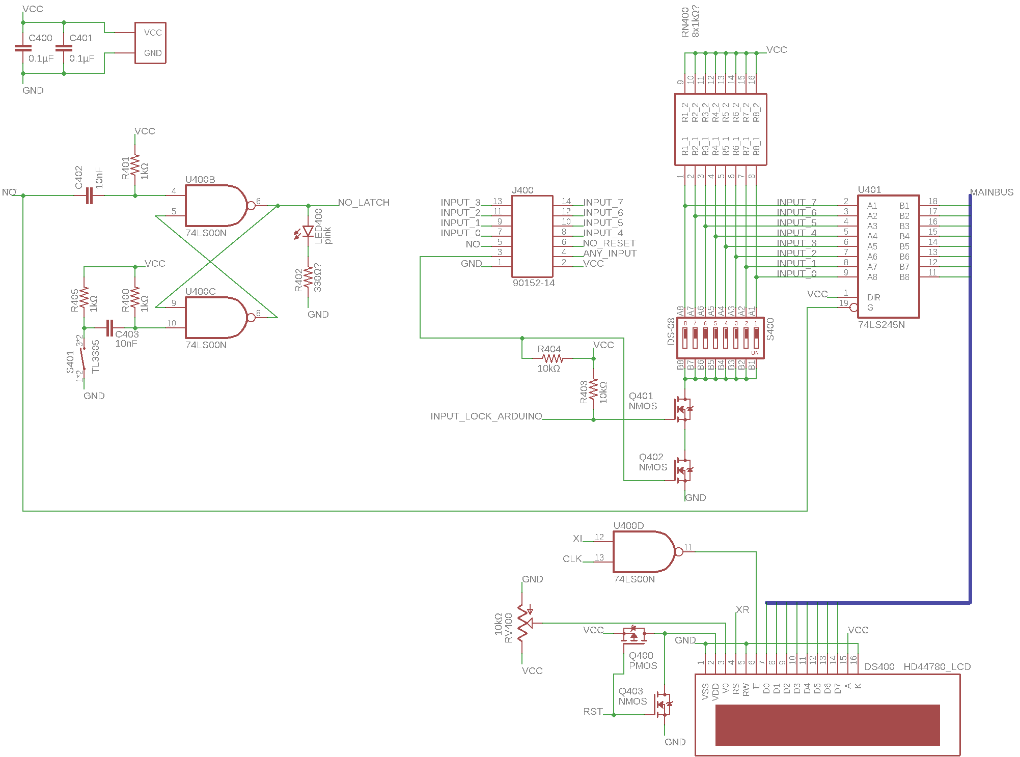
These two modules are relatively simple additions that greatly improve the practical abilities of the computer. Let’s start with the LCD module (bottom).
The main part of it is, of course, the LCD panel itself. I used a typical 16×2 character LCD display with a blue LED backlight. It has an HD44780 controller (or, more likely, a Chinese clone of it). That controller is ideal here, as it has an 8-bit parallel data interface that I can just directly connect to the main bus.
The only things left to connect were contrast (potentiometer on the left), the enable signal (enabled when the LCD is selected and a clock pulse occurs), the register select pin (just another control line), and power/ground. The positive power supply is buffered through a CMOS inverter (two transistors) and is briefly turned off when the computer is reset. That is the easiest way to make sure that the LCD is cleared and reset whenever the computer resets.
The user input module features the input switches themselves (S400, right), with pull-up resistors, and a bus transceiver for output. Alternatively, input can be supplied from the Arduino (see RAM module in part 2), or from an external connector (J400, middle of the page).
To the left of the module, you can see the input enable latch (made of two NAND gates). It’s a simple SR-latch (set-reset-latch) that gets set when the user input is enabled (control signal NO). This lights a pink LED that signals that it’s waiting for input, and pauses the clock to give the user time to submit their input. The user then presses a button (S401) to reset the latch, resuming the clock and allowing the computer to read the input.
Numerical Output
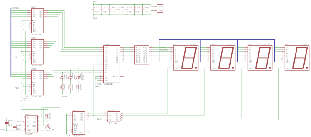
This module also exists in Ben’s computer and is very similarly designed. It’s a simple seven-segment display that can show an 8-bit value in different representations.
On the left side there are three 4-bit register chips. Two of them form an 8-bit register to store the value to be displayed, and the third one stores a 3-bit value that selects the display mode. Currently only modes 000 (decimal unsigned integer) and 001 (decimal signed integer) are implemented, but I could add things like hexadecimal or binary display options.
On the bottom is a fast 555 timer connected to a 74LS161 4-bit binary counter. This is used to quickly switch between the four displays. What this means is that really only one of the four digits is being displayed at once, but it quickly switches between them so that it looks like all of them are lit constantly. This is also called “multiplexing”.
In the middle, you can then see the last part of the display driver: The combinational logic. The inputs are the value to be displayed, the index of the currently lit digit, and the selected display mode. From that, you can determine which segments of the digit should be lit, which are the outputs of the combinational circuit. Instead of creating a circuit out of logic gates, it’s possible to use a ROM (read-only-memory) chip and store the correct outputs for each combination of inputs in the memory. Here, I used an AT28C64B ROM chip.
Continued in Part 5.
Leave a Reply