Let’s start going through the modules of the 8 bit computer.
The Clock
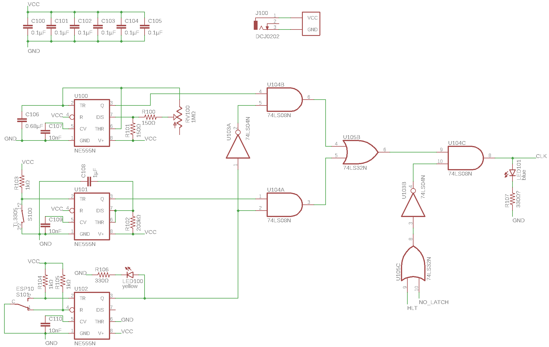
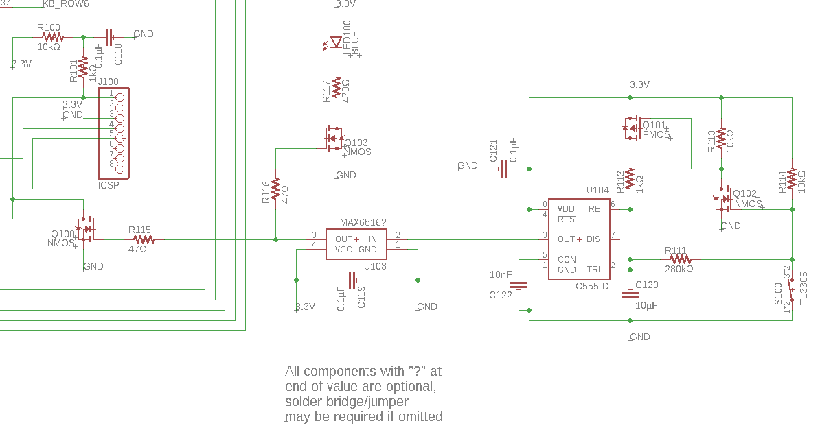
This is one of the few modules that I barely changed from Ben’s design. I only tweaked some of the passive component values and introduced a second signal which pauses the clock. Here’s a quick overview:
The three NE555 timer chips each do different things. U100 at the top works in astable mode, which means its output is constantly oscillating between low and high. This is used for the main automatically running clock of the system. The frequency of that clock signal can be controlled by the user using the variable resistor RV100, that way you can freely choose how fast you want the computer to run.
U101 runs in monostable mode, which means its output is off until it receives a trigger signal from the button S100, at which point the output turns on for a set period of time, then off again. This is used to allow the user to manually input individual clock pulses for debugging and demonstration purposes, while also filtering out switch bounce effects.
U102 runs in a bistable mode, which means its output essentially mirrors the state of the switch S101. The only reason it’s there (instead of just using the switch by itself) is to filter out switch bounce (see above). The user can then flip the switch to choose between the auto-running clock and the manual clock pulses (the latter of which effectively pauses the computer, allowing single steps to be made).
There are also two signals which, when either of them is high, will block any clock pulses from being generated. Those are the HLT (halt) signal that’s set when the computer has finished execution of its program, and NO_LATCH which is set when the computer is waiting for user input (see the User Input module in part 4).
If you want to learn more about the clock, watch Ben’s videos about it.
The A, B, V & F Registers
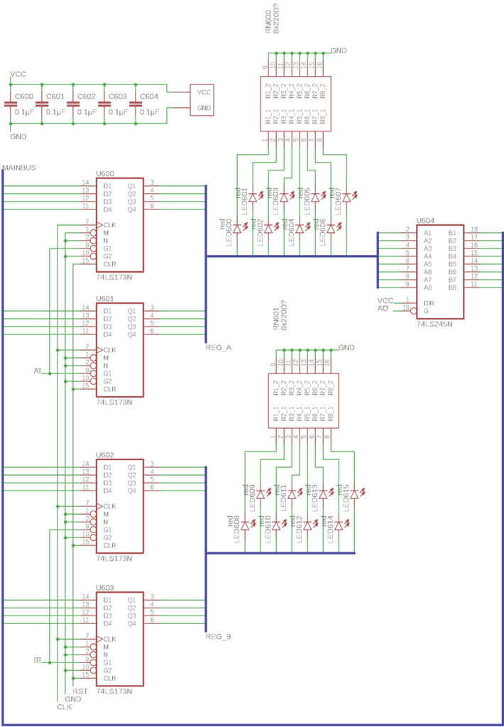
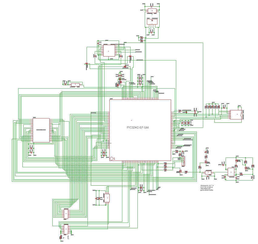
Schematic page 6: A & B Registers 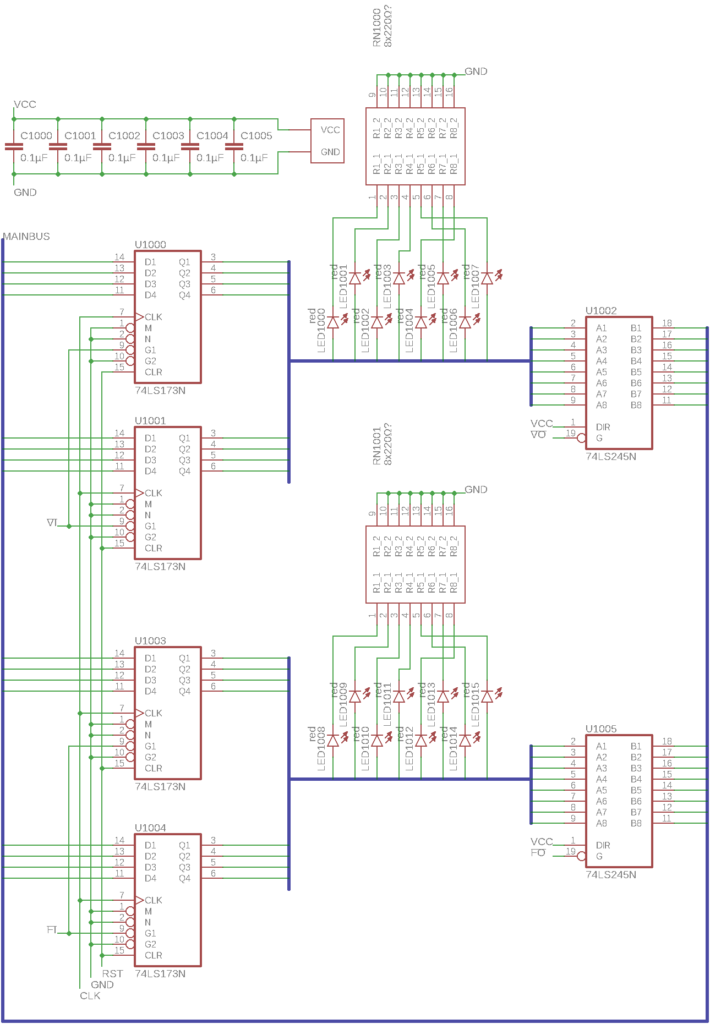
Schematic page 10: V & F Registers
Now let’s look at a very basic component that exists in pretty much any processor: Registers. They are very small, but very fast pieces of memory that are used to buffer data for the processor to work with. These four registers each store 8 bits (1 byte) of data and are used for specific things:
The A register is referred to as the “arithmetic accumulator” or just “accumulator”. It is used both as source and target of many operations. For example during an addition, it contains one of the summands and then gets overwritten with the sum.
The B register is used as the second operand for most operations. To complete the example above, the “add” instruction performs the addition A + B and stores the result back in A. To save some space and control signals, the B register can only be written, but not directly read by the program. (If you really need to read the B register, you can just add 0 to it and you’ll get the “result”, which is the value of B, in the A register.)
The V register is a general purpose register that the programmer can use as they please.
The F register is a hidden register, so it cannot be directly accessed by a program. It is instead used internally by many instructions as a “parking space” for a value that may not be directly available later, for example for swapping the contents of two registers.
Each register consists of two 4-bit register chips (74LS173), eight LEDs to show the register contents with an octuple resistor array to limit the LED currents, and a 74LS245 bus transceiver that allows the register to output its value onto the main bus (with the exception of the write-only register B, which is just missing the bus transceiver).
The A and B registers exist, with the same purposes and design, on Ben’s computer.
Continued in Part 2.