Blog

  • BlockBox v1: Electronics

    One reason why I initially dismissed a Bluetooth speaker project as “too complicated” was, put simply, the Bluetooth part of it. At the time, I barely understood most conventional electronics, so the idea of getting involved with something as complicated as RF communication seemed completely out of my reach.
    Looking back, I was absolutely right about that feeling – trying to design my own Bluetooth receiver would have been a bad idea. Even years later, at the time of writing, I’m not sure I could succeed at that task, unless I spent many more hours researching the topic – and even then, it would be quite a lot of work for a single person, due to the hardware and software complexity involved.

    In light of this, there was only one thing that made me feel confident in pursuing this project anyway: Discovering the existence of Bluetooth audio modules – in particular, for this project, it was the Microchip BM62.
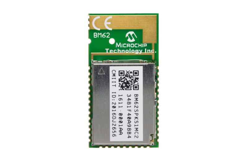
    I found that such a module struck the perfect balance: It satisfied my desire to have the system be “designed by me” to an acceptable degree, while abstracting away the complicated task of maintaining Bluetooth links and sending/receiving wireless audio data, instead providing a relatively simple interface.

    For simplicity, the module has an integrated digital-to-analog converter (DAC), directly outputting the raw audio signal. In my design, this signal would then pass through an analog pre-amplifier and filter circuit, conditioning the signal to the levels I wanted and implementing the driver cross-over (at around 5000Hz).
    The last amplifier stage included trimmer potentiometers, allowing me to adjust the maximum output levels, in order to not overdrive and damage the speaker drivers.
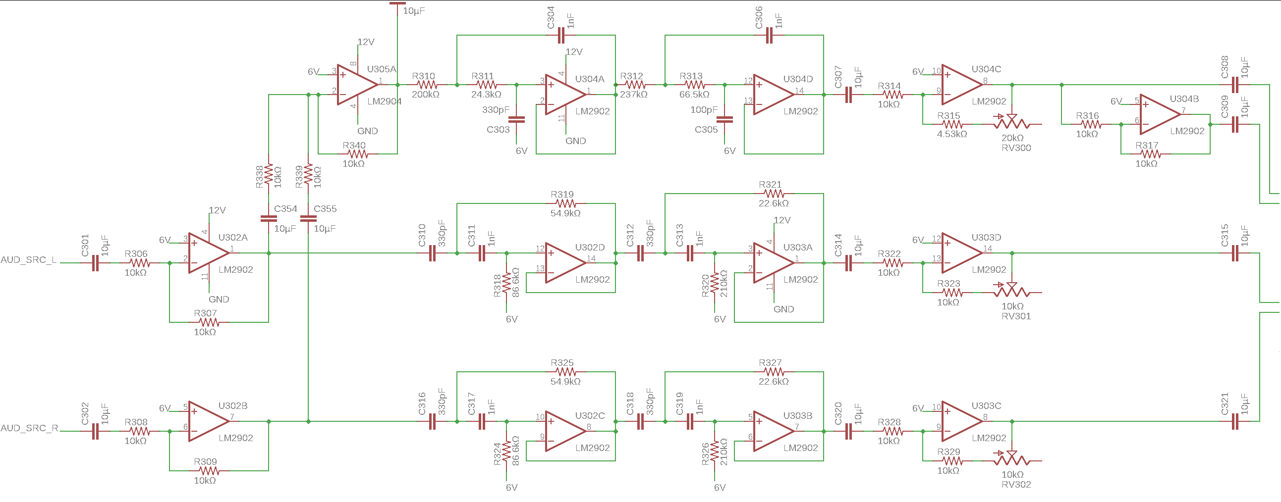
    Looking back at it, this was not a great design by any means – the op-amps I chose are quite noisy, I was using Class-2 ceramic capacitors (which cause distortion), the voltage supplies were not designed with noise reduction in mind at all (likely the biggest single mistake I made here), and so on. But, despite that, it did still work – which is all that mattered to me for this first design.

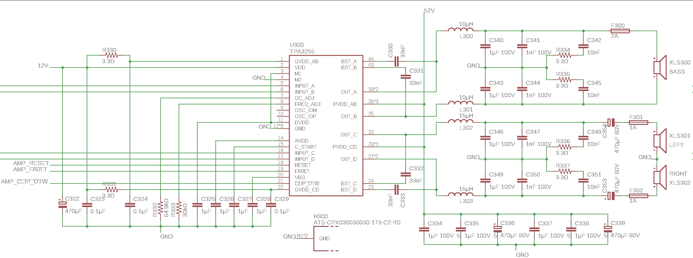
    The pre-amp/filter stage was followed by a power amplifier – namely, the Texas Instruments TPA3255. It was configured in 2.1 channel mode, with two single-ended channels for the tweeters and a differential high-power channel for the bass/midrange driver.
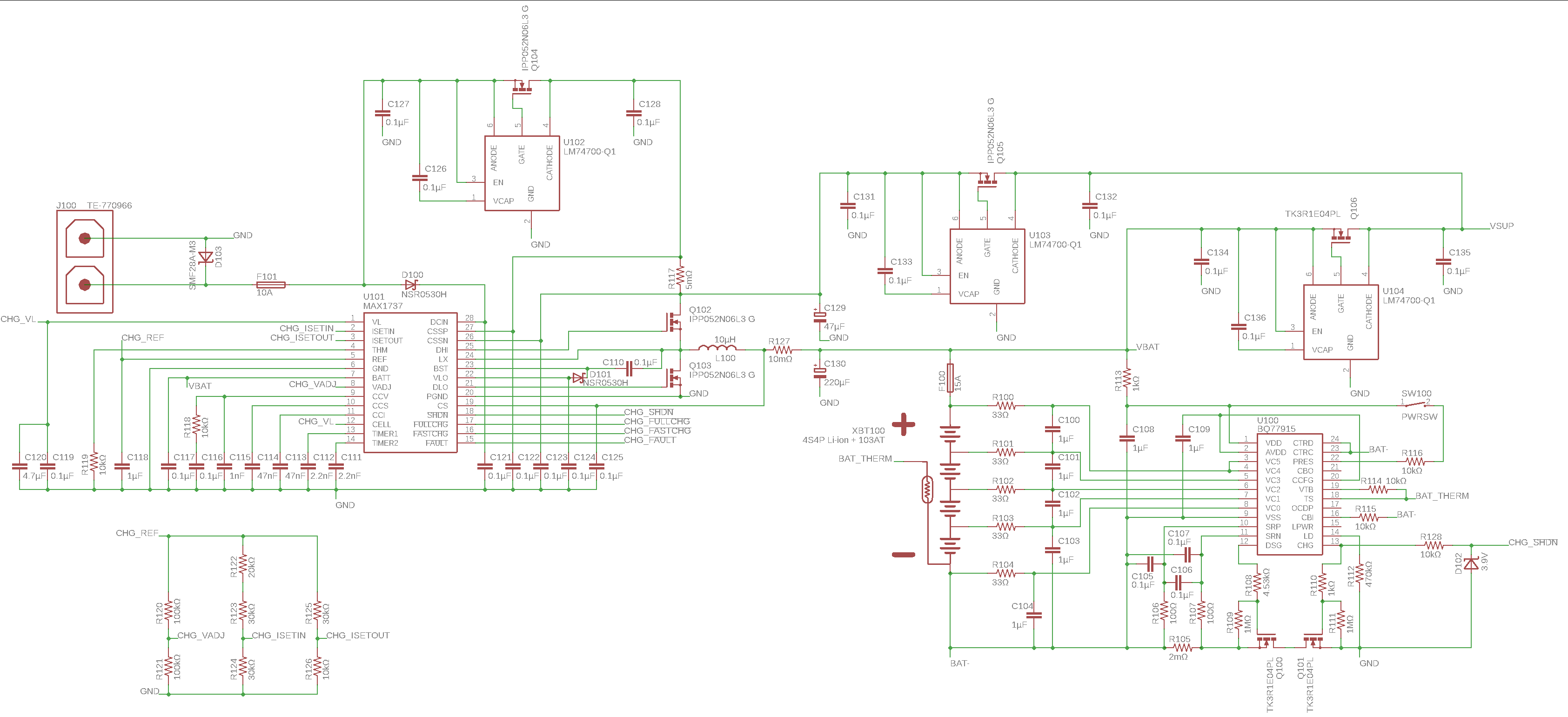
    Aside from the audio path, I needed a power supply. This was based on a large lithium battery (4s4p configuration), with corresponding battery protection, balancing, and charging ICs.
    With the base battery/adapter voltage available, I now needed multiple voltage converters to generate the various system voltages (3.3V, 5V, 12V), as well as a high-power voltage rail for the power amplifier (52V, which turned out to be overkill for these drivers).
    For the design of these converters, the Texas Instruments WEBENCH Power Designer proved invaluable, especially for a beginner without any switching power supply design knowledge.

    For controlling the speaker, I again decided to go with the easiest option, letting the Bluetooth module’s integrated controller operate on its own, controlled using a set of buttons.
    Aside from that, I just added a low-performance microcontroller (Microchip PIC18 K42 series), to handle auxiliary tasks like battery charge estimation, diagnostic display (using a text LCD), and controlling some RGB LEDs that I wanted to sync to the music.

    Since I only had a soldering iron available (no hot air or reflow tools), I ended up being quite limited in terms of component selection. Thankfully, I was able to find everything I needed in “soldering-iron-friendly” packages, but it did mean choosing suboptimal components in many cases.

    Some design work later, I placed and routed everything onto a single 12 x 12 cm PCB.
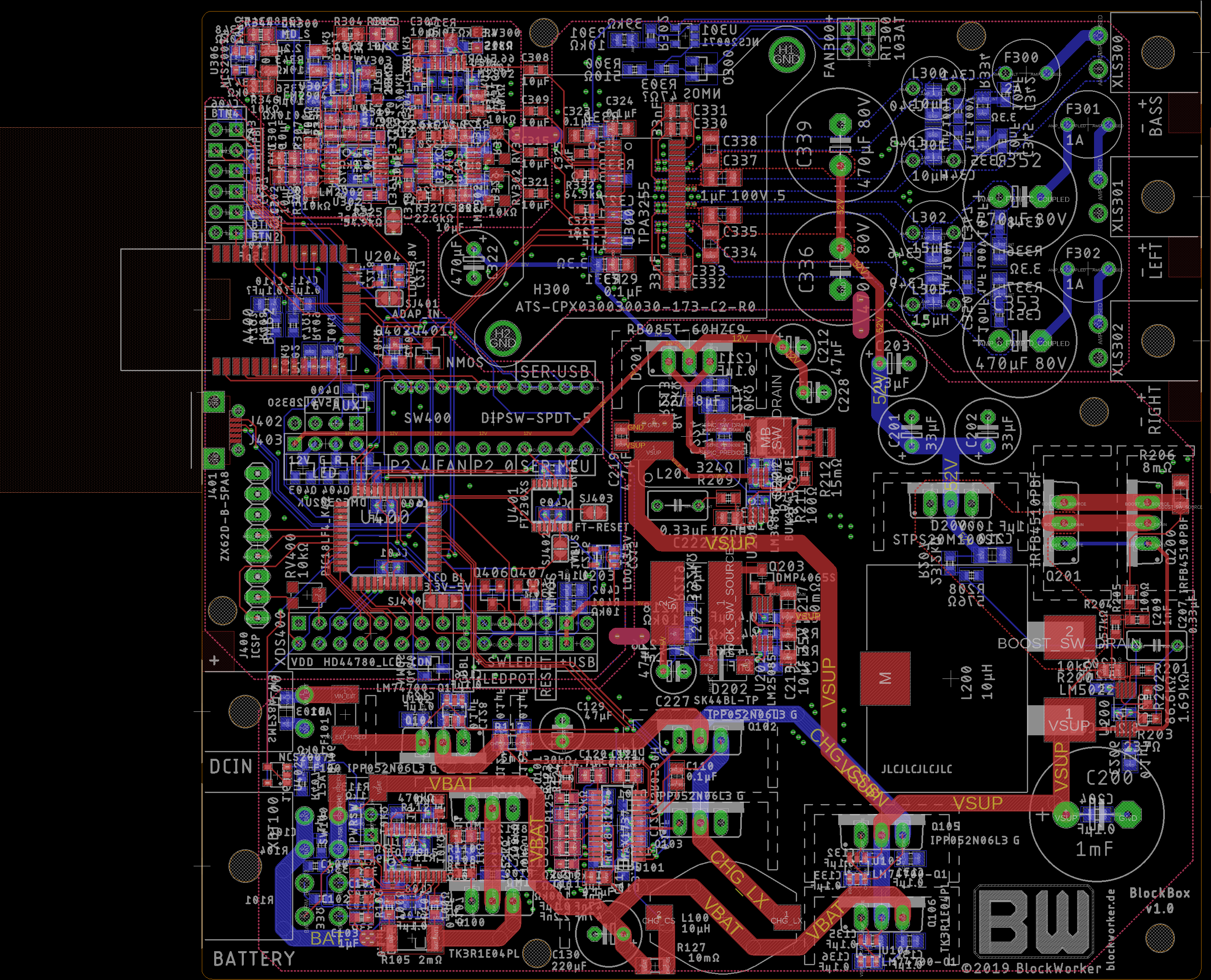
    The full schematics and PCB design files (for Autodesk EAGLE) are available on GitHub here.
    However, be aware that this design is NOT GOOD overall, containing many beginner mistakes, and the firmware code quality is likely bad for the same reason. Therefore, I do not recommend that anyone actually use these designs, but they may be useful for anyone who’s curious.

    With the electronics designed, it was time to begin the actual build!
  • BlockBox v1: Speakers and Enclosure

    As I started my research into designing the BlockBox, I realised one thing: Speakers are really complicated.
    So many speaker drivers to choose from, priced anywhere between affordable and astronomically expensive, with different sound profiles, efficiencies, features, and drawbacks.
    And what the hell are “Thiele/Small Parameters”?!

    Hours of research later, I figured out what most of these things mean, and found out that the final size (volume) of the speaker would play a major role in the low-frequency sound design. Since most commercial Bluetooth speakers are very small, I always imagined making one of a manageable size too – so that is what I decided on. It’d still be larger than the typical “handheld” mini-speakers, but small enough to fit in a backpack.

    Finally, I decided on a set of speaker drivers to use for this project. I wanted my speaker to be loud, so driver efficiency was very important, and my budget was quite limited, of course.
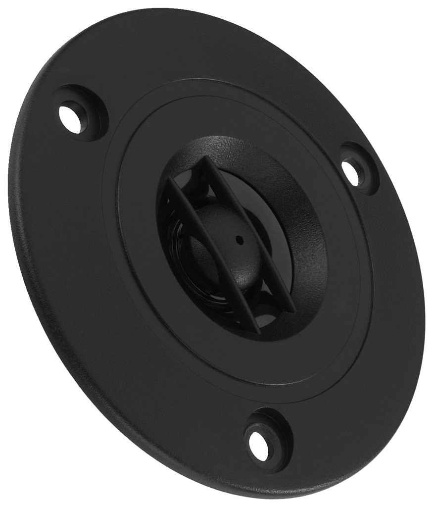
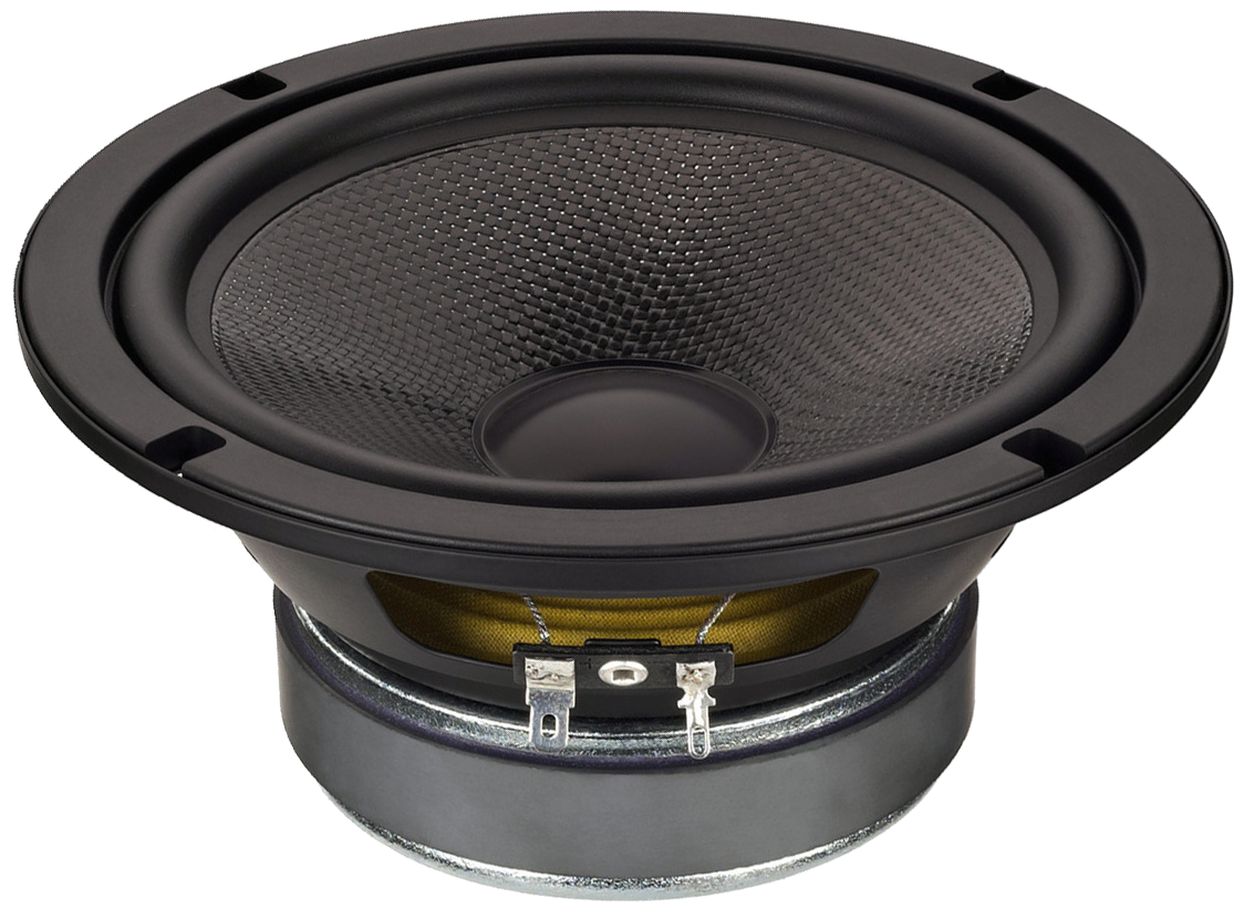
    Therefore, I went for a two-way crossover speaker, using the 6.5″ Monacor SP-6/108PRO as a bass/midrange driver, and the Monacor DT-74/8 tweeter (or, in fact, two of them – mostly for the sake of symmetry, as you will see later).

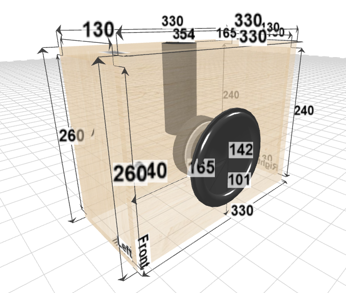
    In order to get the most out of these drivers, the design of the enclosure was quite important. Using SpeakerBoxLite, an incredibly useful free tool for speaker design, I determined that a vented enclosure with a volume of 8.7 litres would be perfect given these drivers and my size requirements.
    Combined with a port resonator of the correct size (Monacor BR-50HP), this results in a 33 x 26 x 13 cm speaker enclosure with 10mm plywood walls.

    According to the SpeakerBoxLite calculations, this should result in a flat frequency response down to 90Hz and a -3dB roll-off point of 72Hz. Not great, especially for fans of music with lots of bass (including myself), but not terrible either.
    I’m sure it’s possible to do better within the constraints of this project, but all better options I found back then were too expensive, too inefficient, or just too complicated for me, as a beginner.

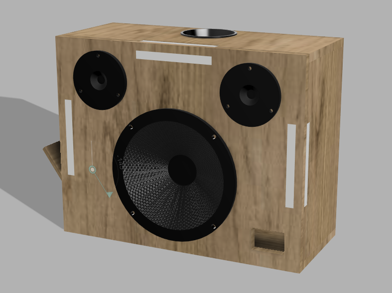
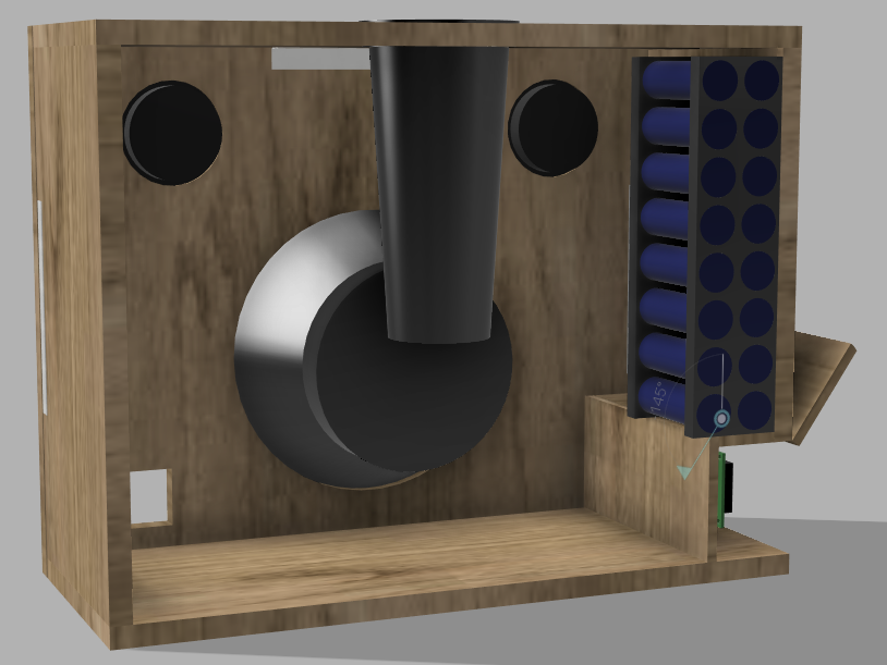
    Based on this rough sketch, I created a more detailed enclosure design in Autodesk Fusion 360 – featuring all drivers, some translucent bars for LED lighting, a cutout for buttons to control the speaker, a side compartment to house a diagnostic display, the main power switch, and connectors for charging etc., and of course, enough space in the back for the battery and electronics.

    With that out of the way, it was time to move on to the electronics design.

  • The BlockBox Project

    The BlockBox Project

    Before I even started my first electronics project ever around 2017 (at age 16-17), I already had an idea on my mind: I wanted to build my own Bluetooth speaker someday.
    Why? I’m not sure myself. Maybe it was just a naive ambition of a curious teenager, maybe I just wanted to look cool at parties as “the guy who built his own speaker”, or maybe there was something else that interested me about them.

    As I was starting out with no real electronics experience and very limited knowledge, the idea of building an entire speaker by myself seemed nearly unattainable.
    I would have probably been able to make something by buying and chaining together pre-built modules (battery management, Bluetooth receiver, amplifier, etc.) – but this approach, while quite popular in beginner DIY/maker spaces, has never felt appealing to me. It just felt like it wouldn’t really be my project, but just an amalgamation of others’ (commercial) projects.
    Therefore, I put the idea aside, though it never left my head entirely.

    Eventually, in 2019, I felt ready to try my luck at actually building such a speaker, from the ground up. And thus, the BlockBox project was born.
    Looking back, I was still naive and clueless about a lot of the intricacies involved, but despite that, I feel it would be wrong to call the project anything but successful.

    Start here to read the full story of the BlockBox project.

    All chapters
  • The 8 Bit Computer – Conclusion and Outlook

    With that, the 8 Bit Computer project was essentially finished.

    This was my second large electronics project, and it was a lot of fun to work on. It’s difficult to consider it “completely done” (some minor issues and optional improvements remain), but I decided I’d call it done and maybe get back to it later – though that seems to be a recurring theme with all hobby projects, at least in my experience.
    Also, none of these imperfections change what this project is: A fully functional basic computer that, in my opinion, looks great, and is a nice tool to show how computers work on a basic level.

    This project was designed and mostly built before I started my university education in computer science. The experience from it helped me a lot in my first computer architecture courses, as I already knew a lot of the concepts. However, there were many things that I didn’t know prior to taking those courses, and many things I’ve learned about computer architecture that I didn’t know when designing this computer. So looking back at it, there are quite a few things I would do differently if I were to start a project like this now. Still, I am proud of it and happy with how it turned out.

    In the future, I may design a new computer, perhaps implementing some more advanced computer architecture features and avoiding some of the problems that I encountered and worked around in this one. Until then, I recommend everyone who’s interested to keep looking into this topic – there is much more to learn than what I’ve covered here!

    Until the next project!

  • The 8 Bit Computer – Instructions and Programming

    With the electronics finished and working, the computer now needs to be told what to do. This is realised by implementing instructions that perform small individual tasks on the computer, like moving a value between registers or adding two numbers. These instructions can then be combined to create more complex programs.

    Each of these instructions is associated with an opcode (operation code) which is used to identify the instruction in the binary program. The computer reads an opcode from memory, executes the associated instruction, then reads the next opcode, executes that, and so on. This fetch-execute cycle continues until the program ends, i.e., a special instruction tells the computer to stop executing the program.

    To the programmer, the instructions are atomic, which means they are the smallest steps the program can be divided into. However, in this computer implementation, these instructions are subdivided into even smaller microinstructions (as discussed in the “Modules, Part 5” chapter). Each of these microinstructions is exactly one clock cycle long and defines the hardware control signals that should be set for the execution of the desired behaviour. For example, to read a value from memory, first the target memory address needs to be moved to the memory address register, then the value at that memory location can be read. Some of these microinstructions are also used to implement the fetch-execute cycle (read next opcode and pass it to the control logic).

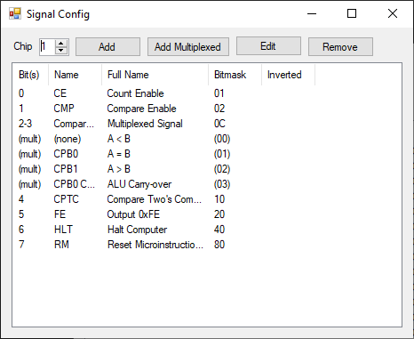
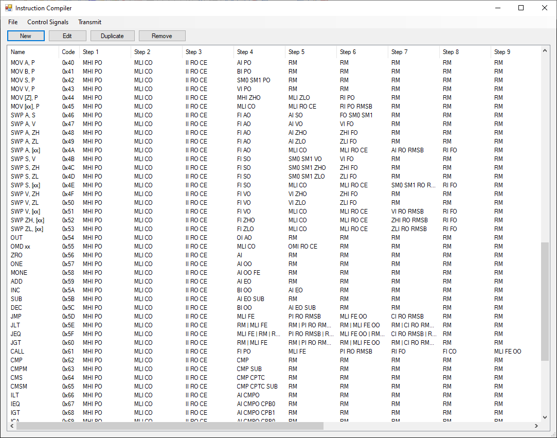
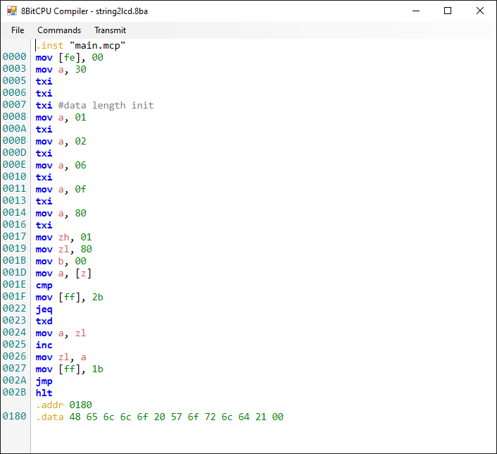
    To manage the programming of these instructions, I wrote an app in C# where you can define the control signals that exist in the computer, use them to program instructions out of microinstructions/steps, and use those instructions to write programs that can run on the computer:

    Control signal configuration window
    Control signal configuration (not all signals shown here).
    Instruction definition window
    Instruction definition and microinstruction programming.
    Assembly programming window
    Editor for writing programs using the defined instructions.

    The instructions and programs can then be written to instruction ROM or computer RAM, respectively, using an Arduino (which is controlled from this same app).

    With this, you can program the computer to do essentially anything that it’s physically capable of with the provided hardware. The program shown in the third screenshot above prints “Hello World!” to the LCD screen (bottom left). Here is a video of it running:

    To avoid waiting too long for the message to appear, the program is running too quickly for the human eye (tens of clock cycles per second), so you can’t really see the individual instructions running – but it is rather spectacular to watch the control signals (white LEDs) going crazy! If you look closely, you can see the “HLT” LED at the right light up pink at the end – this is the “halt” signal that tells the computer to stop running when the program is done.

    So with that, we have a working and programmable computer! In the final post for this project, I will discuss the end result and give an outlook of what may come next.

  • The 8 Bit Computer – PCB

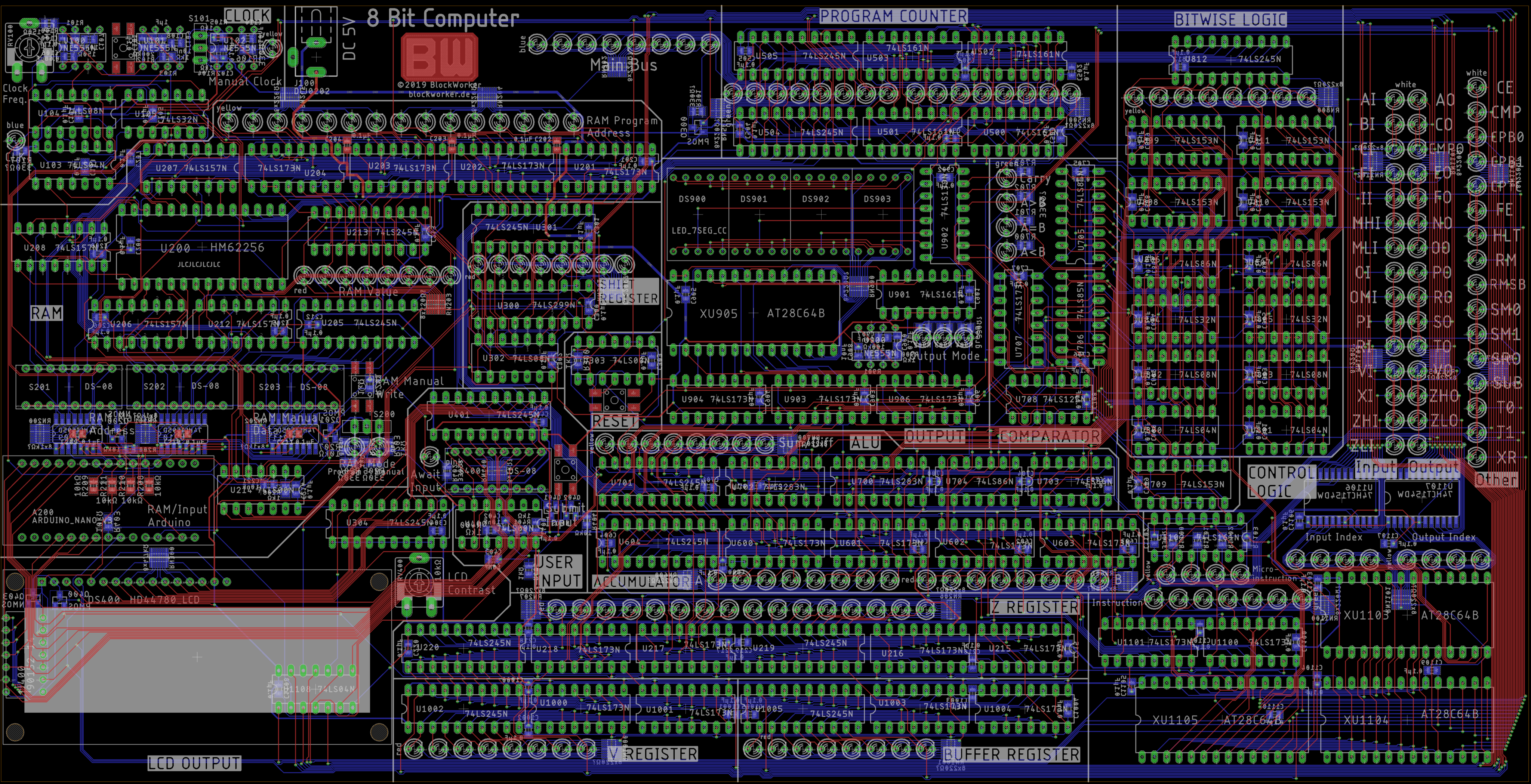
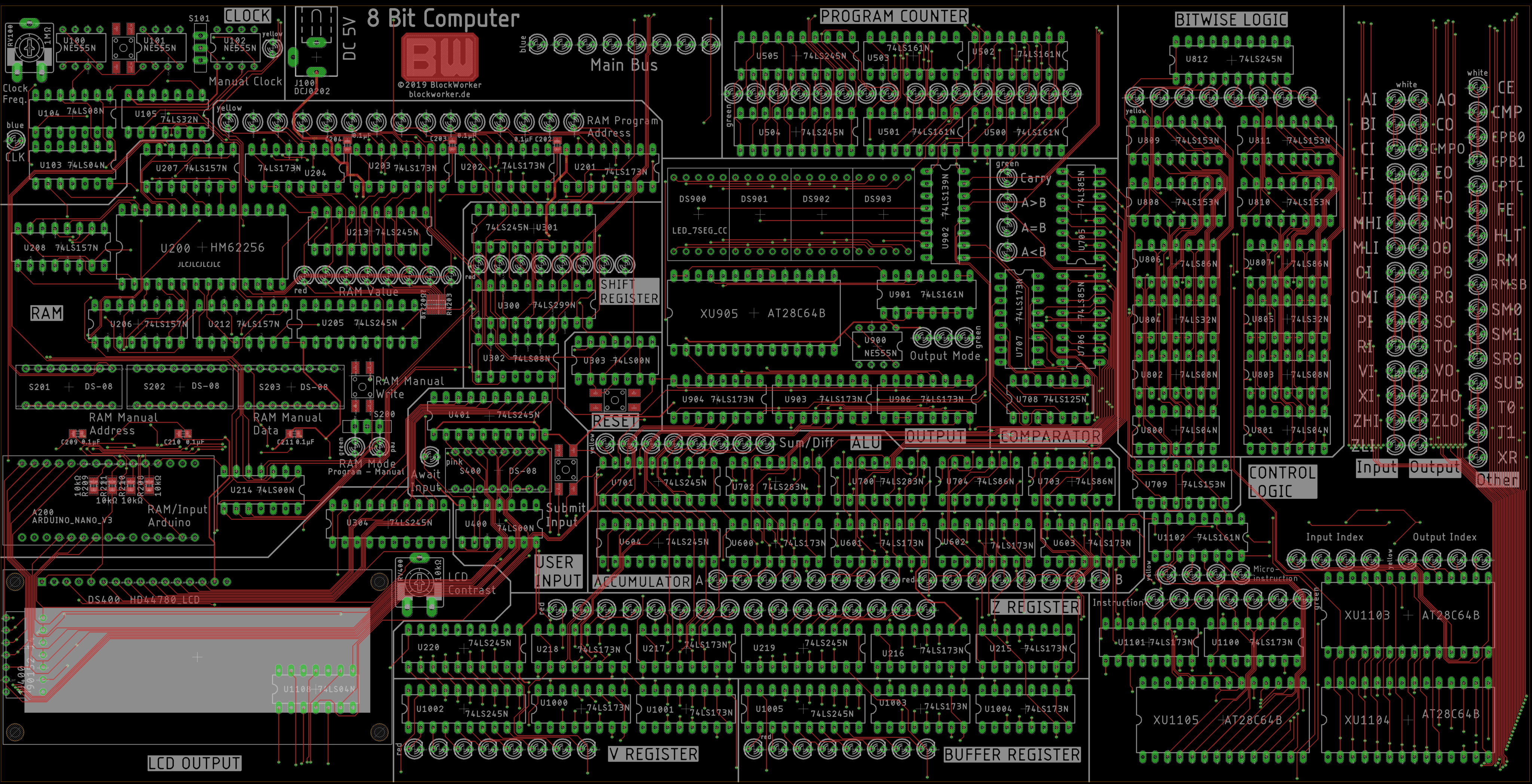
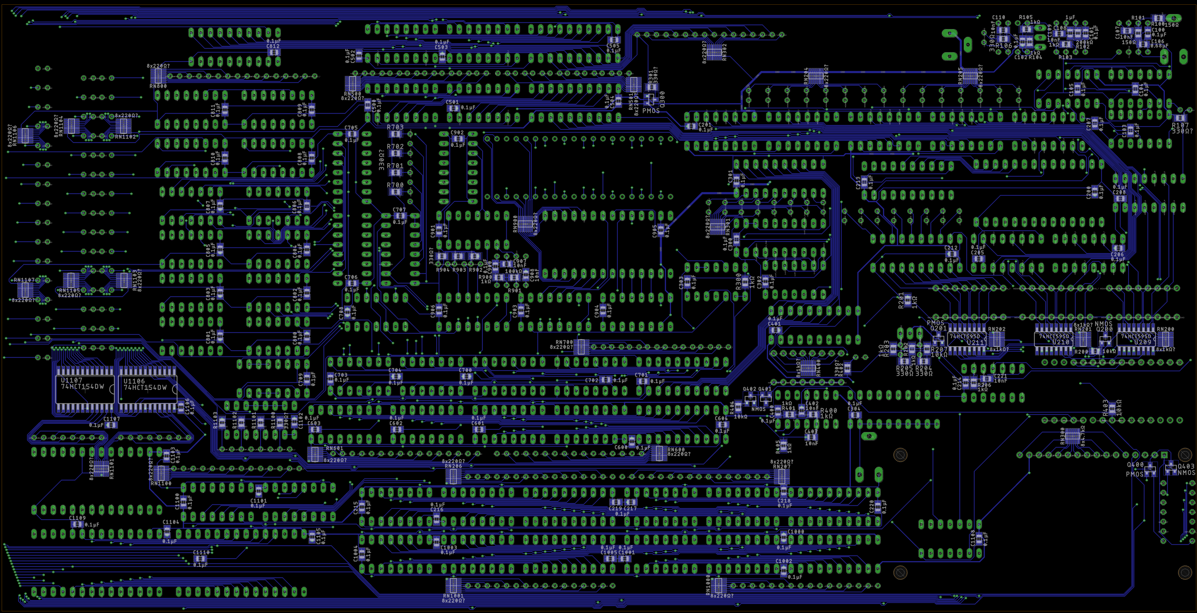
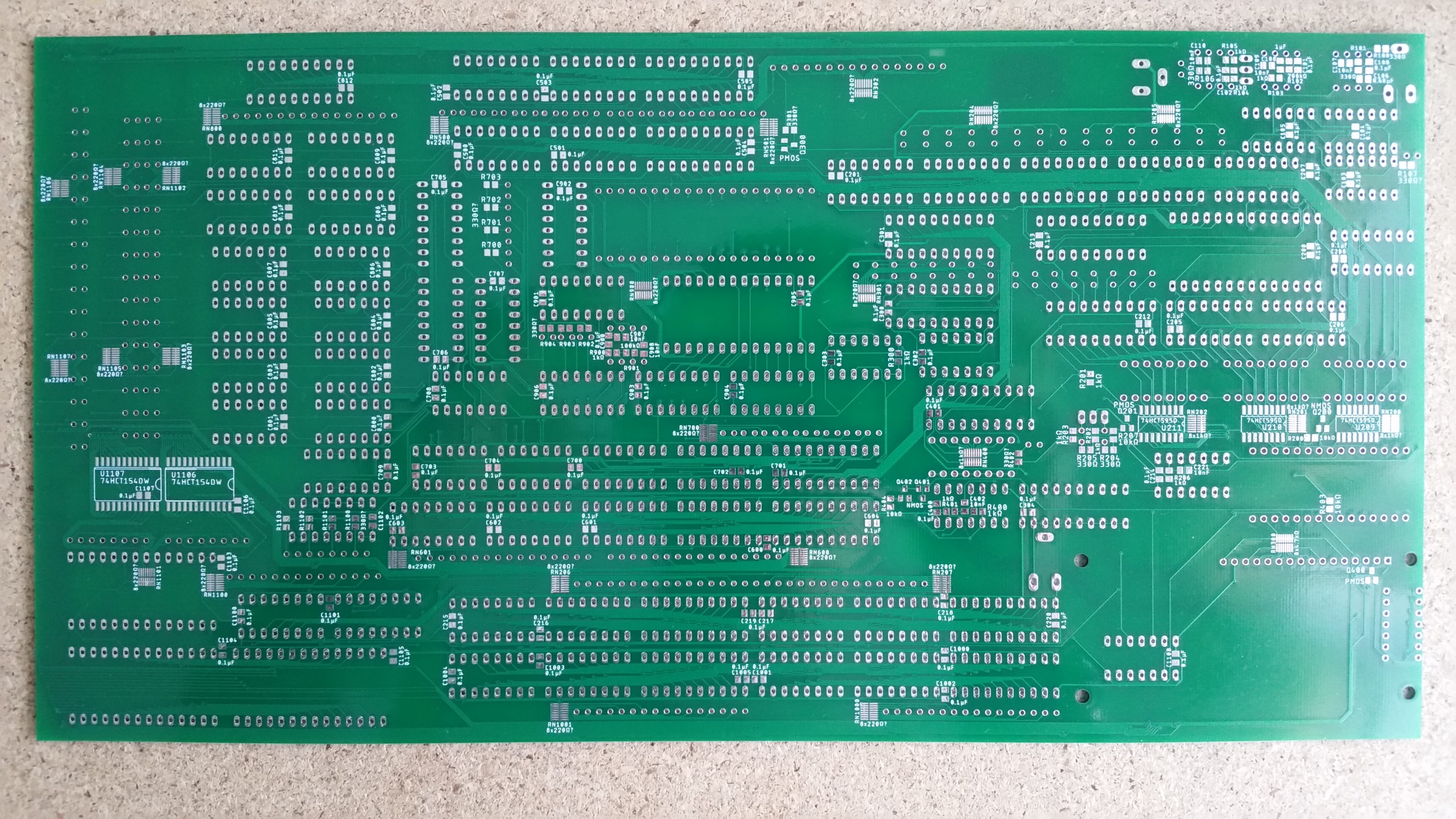
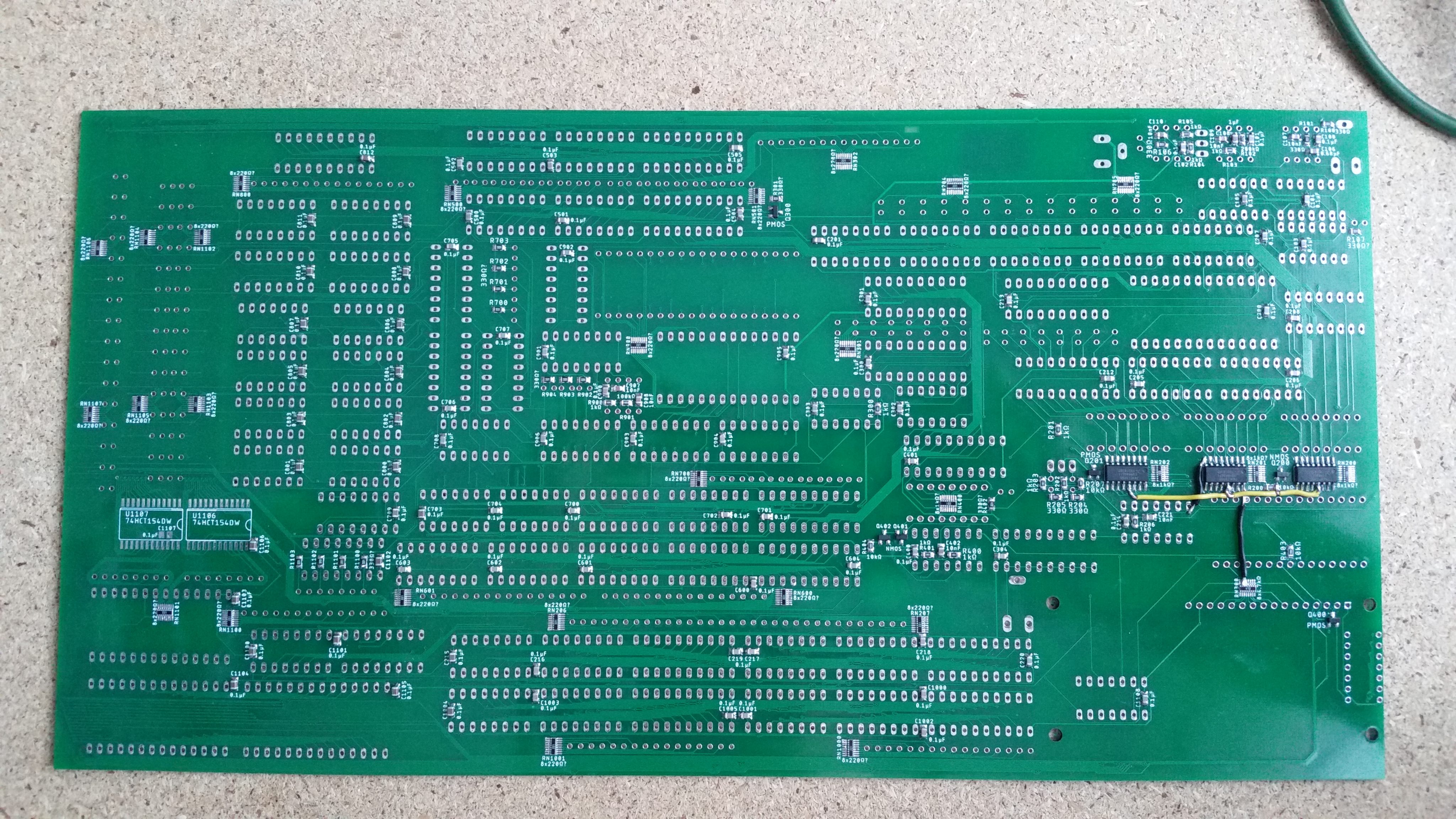
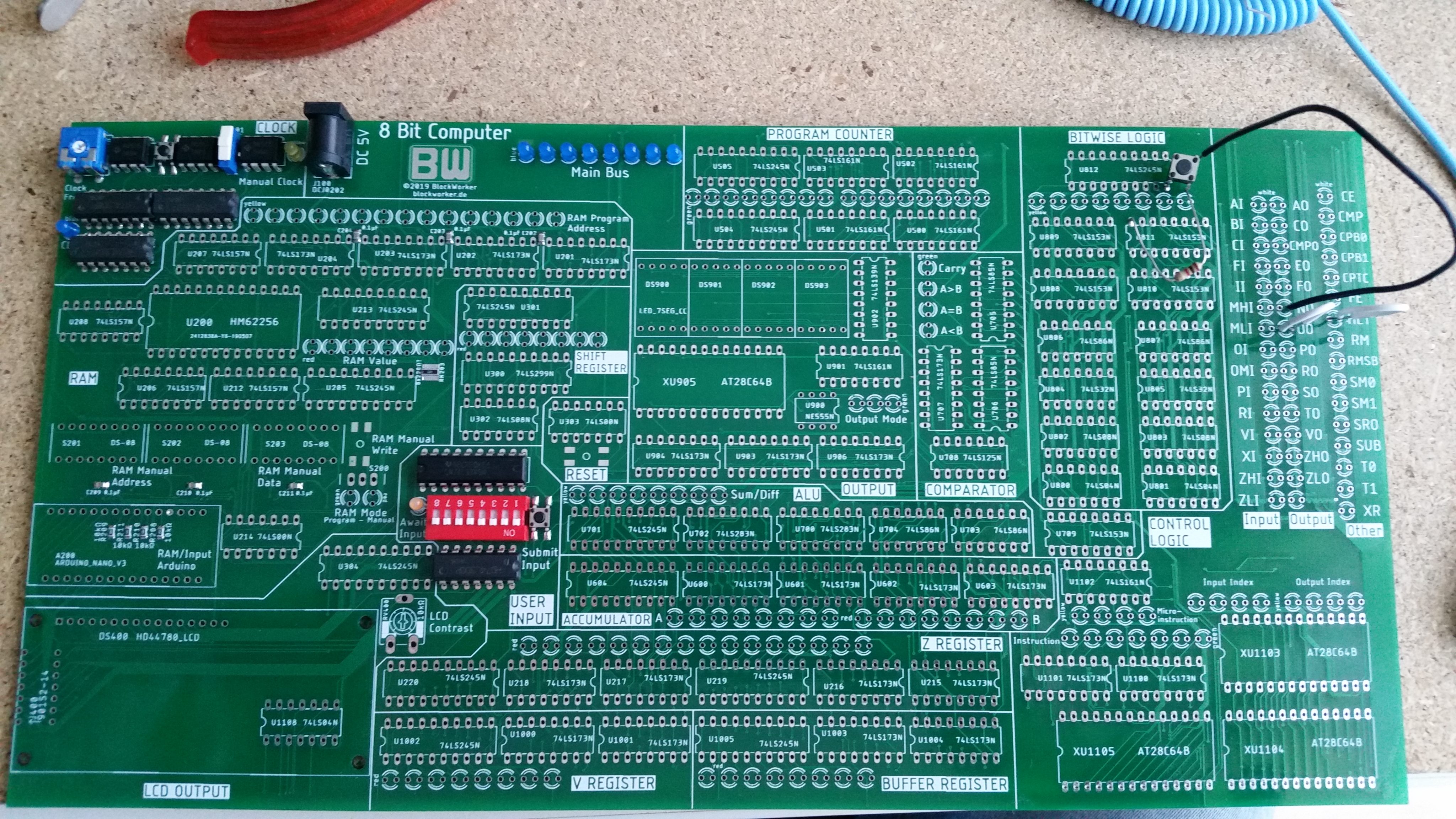
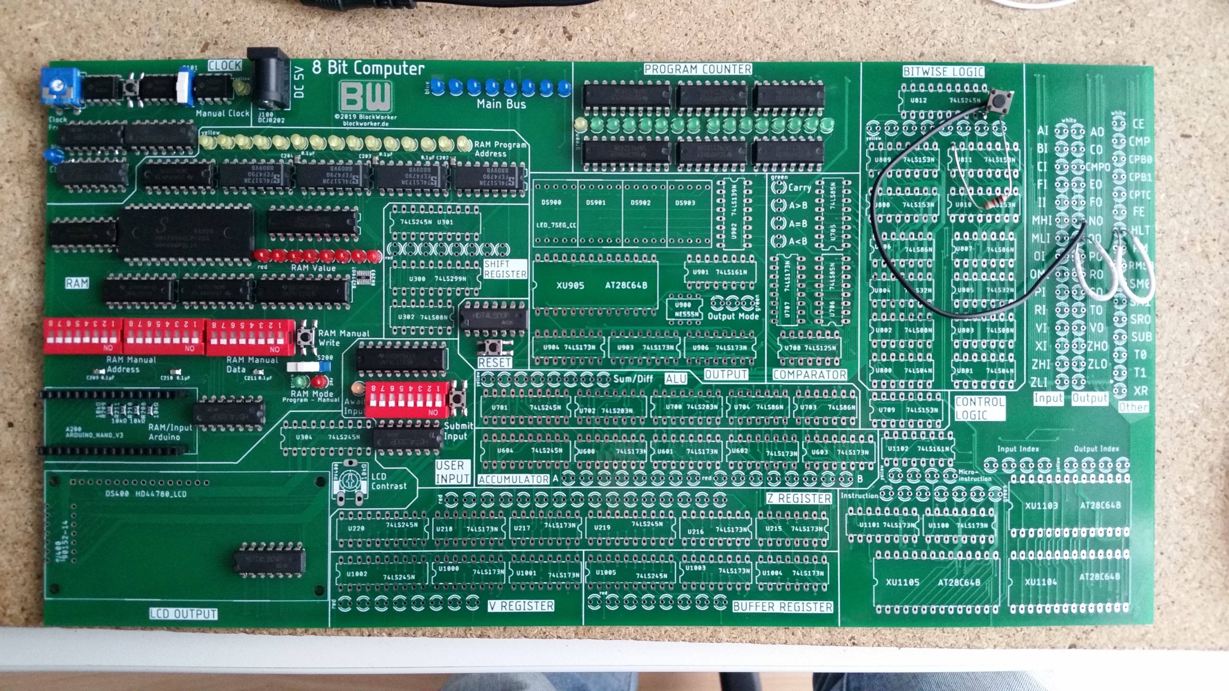
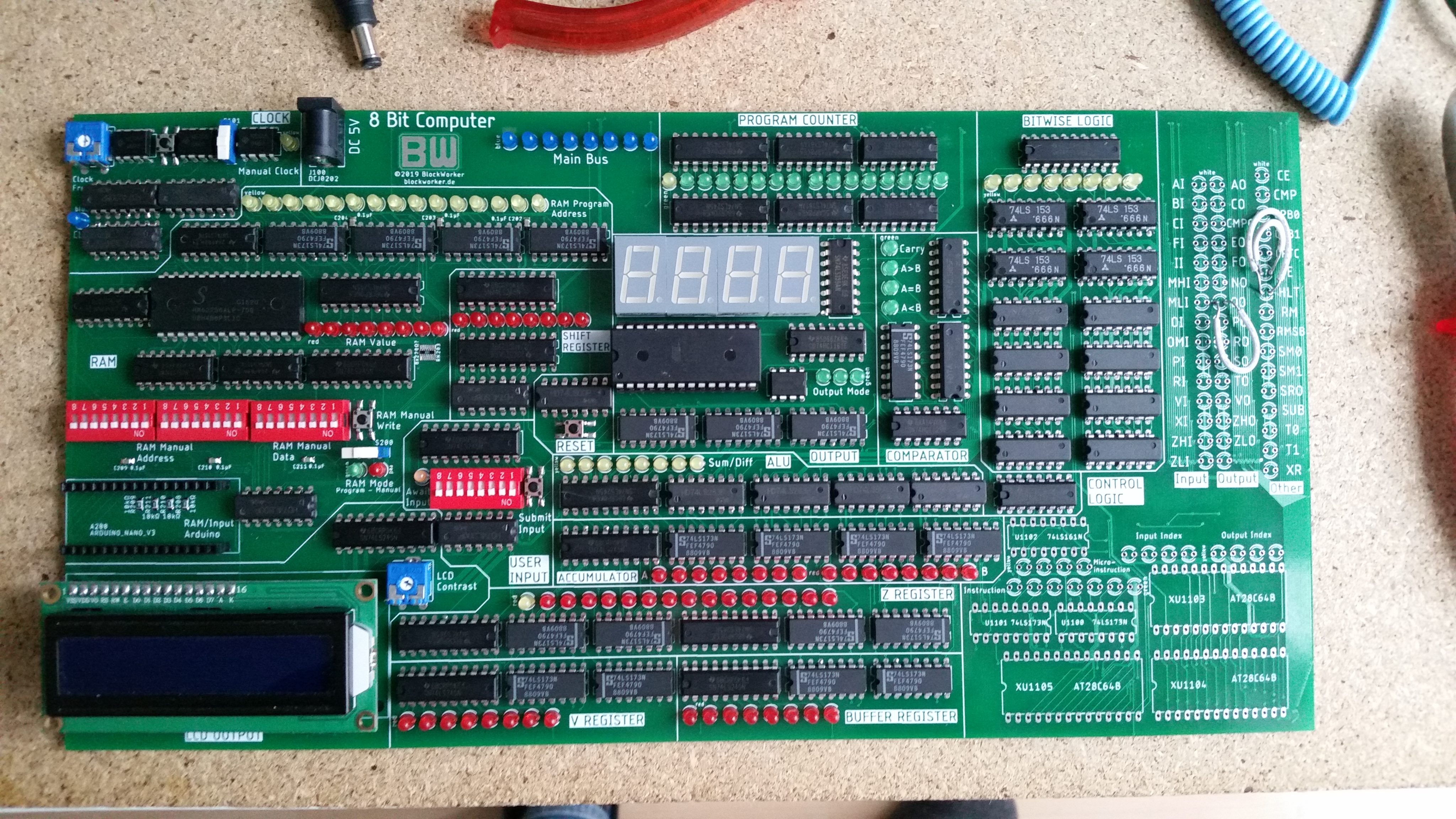
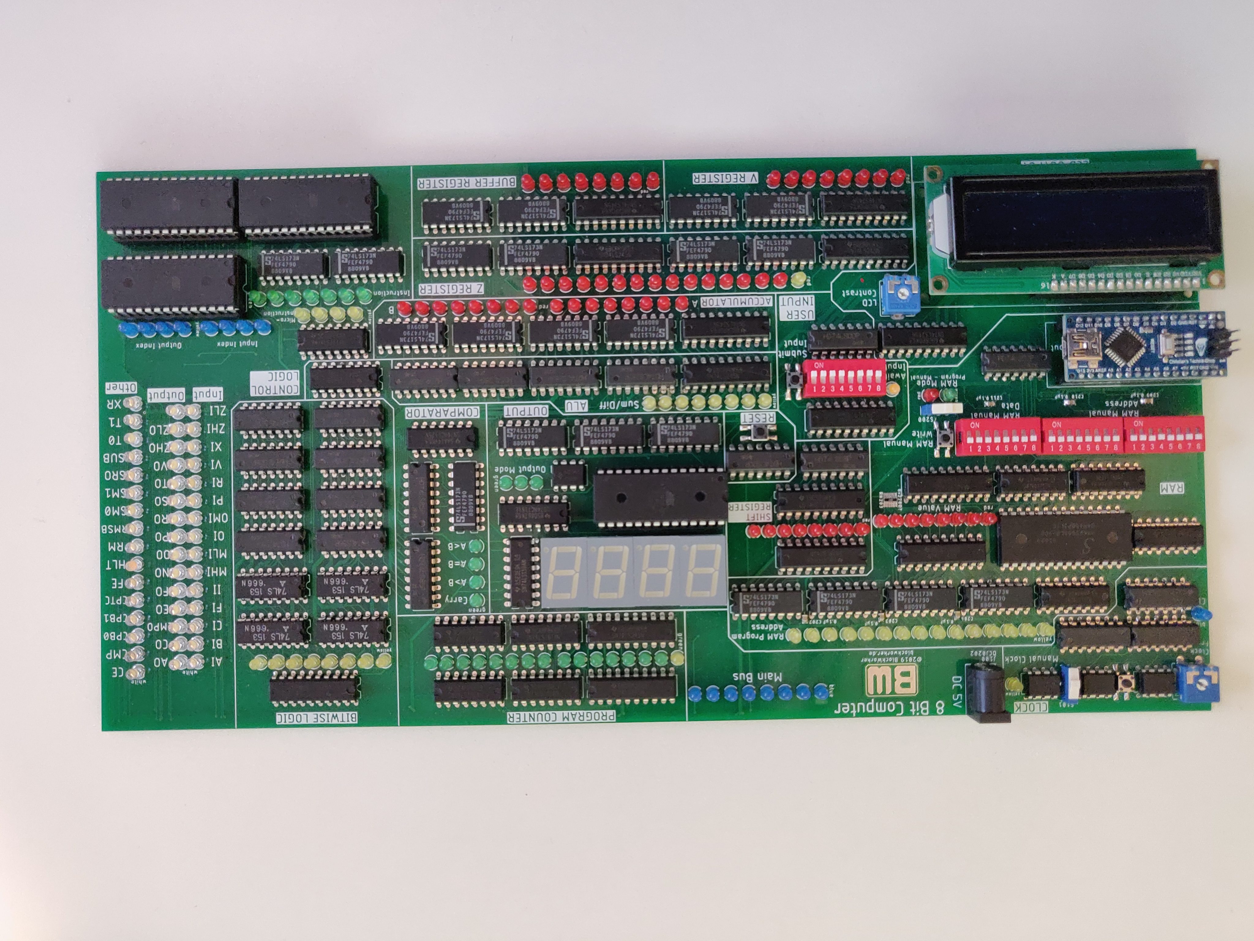
    In the previous posts, I explained the schematics of the different modules of the computer. Based on those, I made a large PCB (printed circuit board). You can click the images to zoom in.

    Total board view (looking through from the top)
    Board top view
    Board bottom view

    As you can see, the board is quite cramped. I wanted to reduce the board size as much as possible, to save costs and make it more portable. This made signal routing quite challenging, as the through-hole component pads (green) don’t leave a lot of room for the over 2000 wire connections required. I also fit it all into 2 layers (top and bottom) – I didn’t want to use a 4-layer PCB, as it’s significantly more expensive (at this size), and I believed that it could be done with just 2. It seems that I was right.
    As expected, given this was my first dense circuit board design ever, it does contain some beginner mistakes – for example, not using any ground planes, and making power/ground traces thinner than ideal. But it’s fine, I learned from it, gained experience with PCB design, and the board did end up working anyway.

    The total board size ended up being 31.5 x 16.1 cm (12.4 x 6.4 inches), which is a lot smaller than I initially expected, considering the breadboard prototype was about 40 x 40 cm (15.7 x 15.7 inches).

    I wanted to keep the individual modules visually separated on the board, to show how the computer is made of these somewhat independent pieces working together. I went through multiple layout iterations for each module, to make it stand out as a separate entity, but still fit in well with the other modules. Additionally, I drew some thick lines on the silkscreen as rough outlines between the modules and labelled them all. The LEDs are also arranged in nice bit strings in the correct reading order, and labelled if necessary.

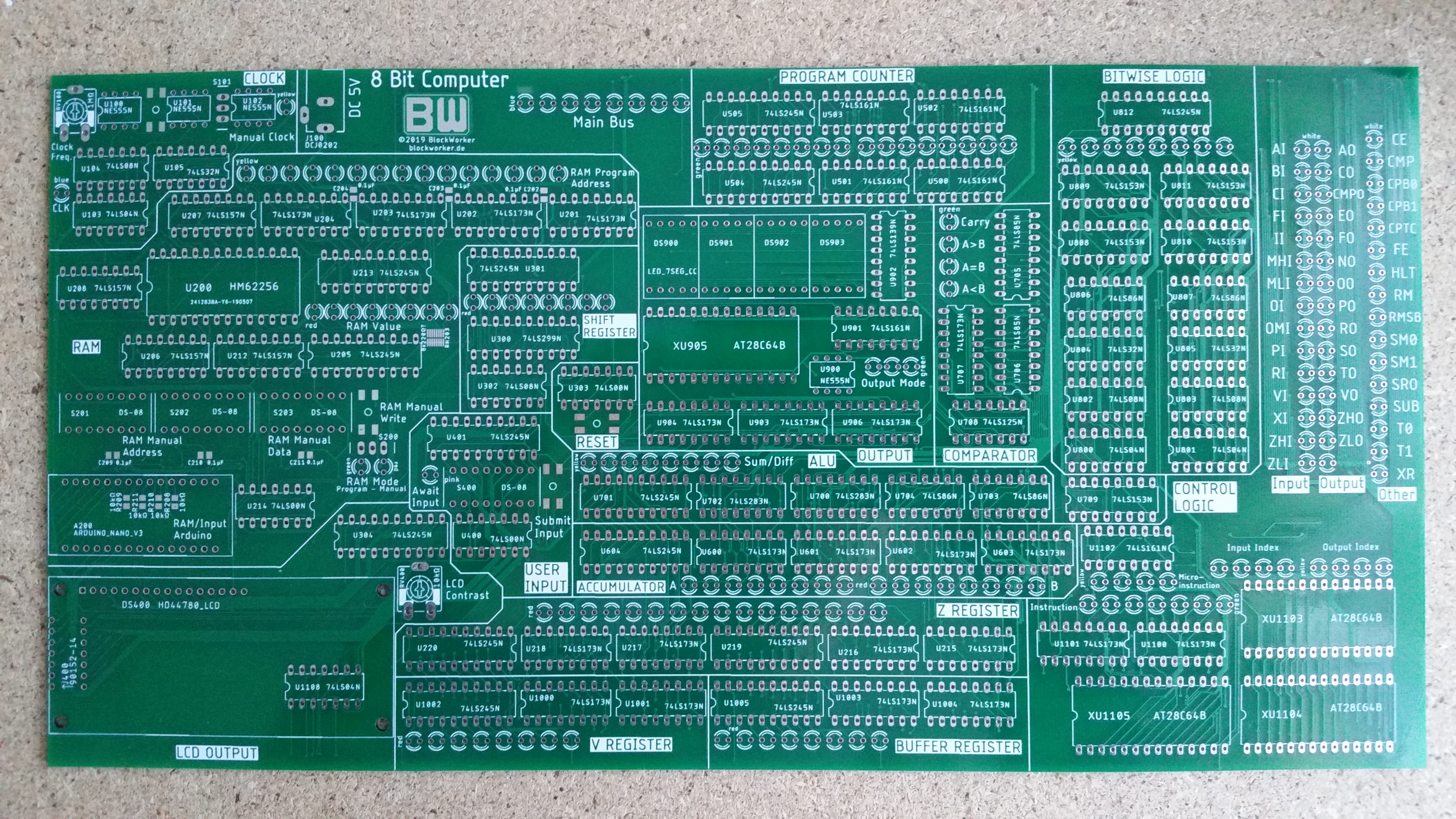
    Here’s the raw PCB, fresh from the friendly neighbourhood Chinese factory:

    Raw PCB Front
    Raw PCB Back

    And here are some impressions from the assembly process:

    Immediately noticed the first PCB mistake… Rather easily fixed though 🙂
    Clock and user input built and tested
    Program counter and RAM modules complete
    Remaining registers and arithmetic modules done
    And finally the control logic.
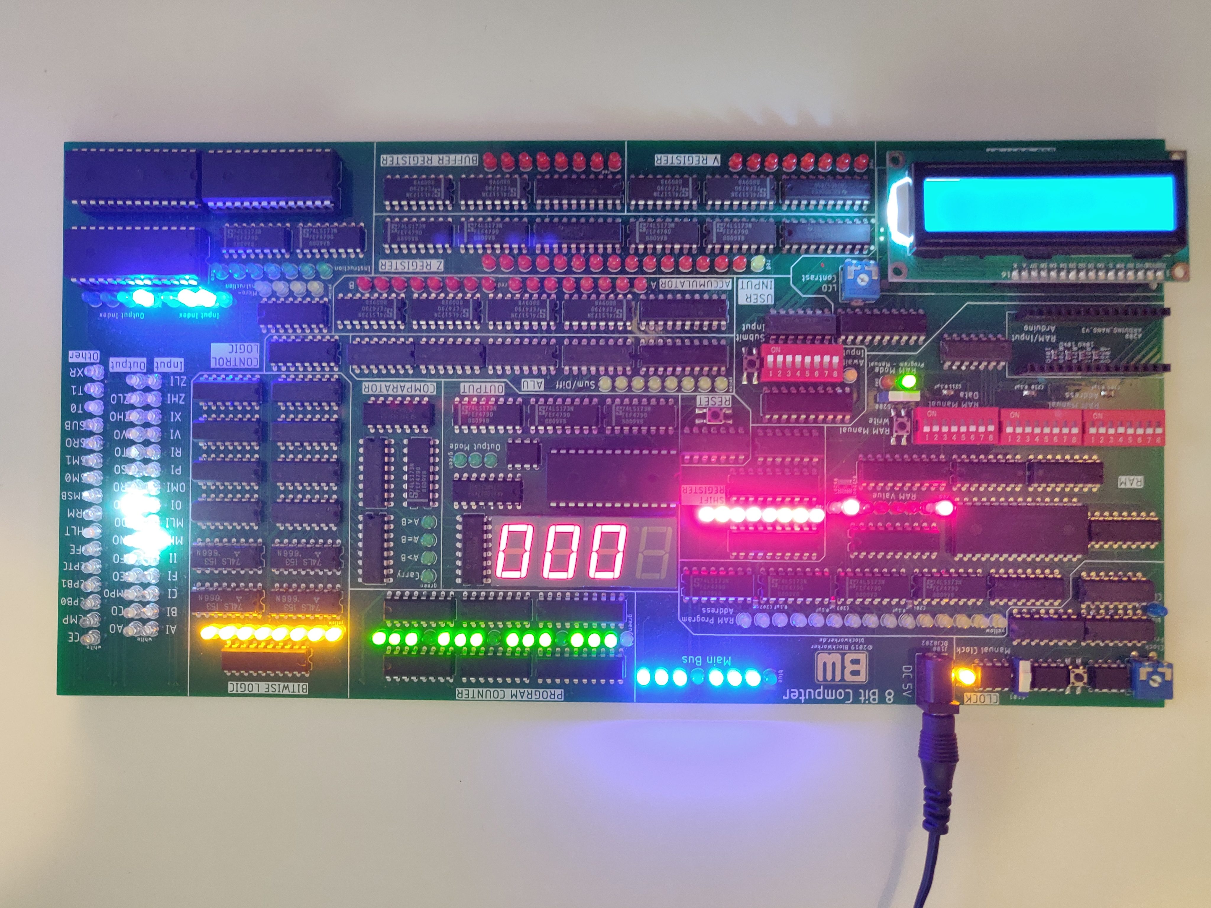
    Initial power up looks good!

    The assembly was surprisingly fast, it only took about a week. Most of it was rather repetitive, soldering thousands of component pins, but seeing it come together felt great anyway.

    Now that the PCB was assembled, there was still one thing missing for the computer to work: Programming the instruction behaviour. This is what we will look at next.

  • The 8 Bit Computer – Modules, Part 5

    Program Counter

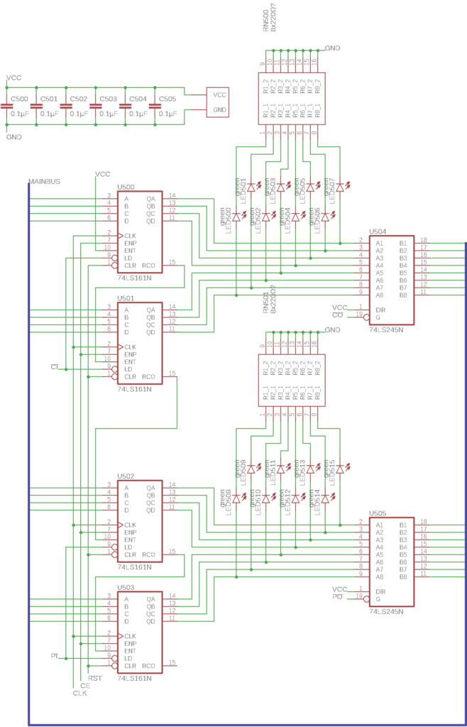
    Schematic page 4: Program Counter

    Another one of Ben’s modules that’s been slightly expanded, the program counter is a basic tool that is required for program execution: The computer needs to keep track of its current position in the running program. That way, it always knows where in memory the next instruction can be found. The program can also overwrite this counter with an arbitrary value, which has the effect of jumping to that point in the program.

    The counter itself is implemented using four 74LS161 4-bit binary counter chips which are cascaded to create one 16-bit counter. As the data bus is only 8 bits wide, the counter input and output is divided into two virtual registers, P (“page”, higher 8 bits) and C (“counter”, lower 8 bits). As usual, the output is managed using 74LS245 bus transceivers, and there are some LED packs to display the counter value.

    Instruction control logic

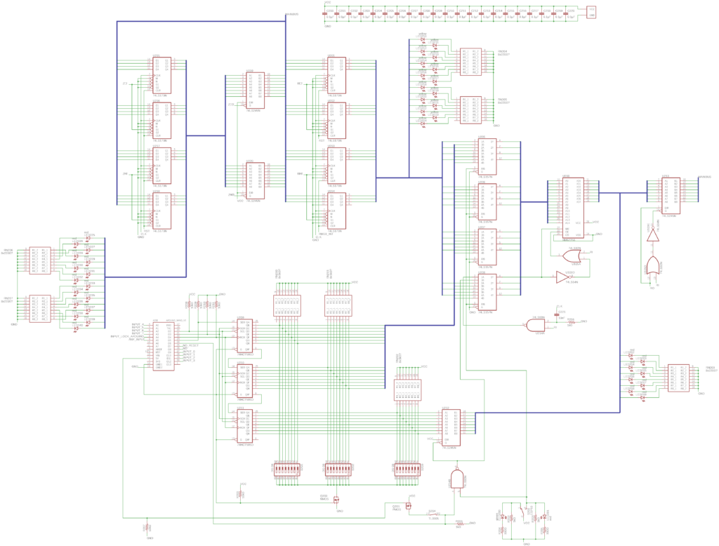
    Schematic page 11: Instruction Control

    Now this module is where the magic happens: It tells all the other modules that we’ve seen what to do and when to do it. Ben’s version can be found here.

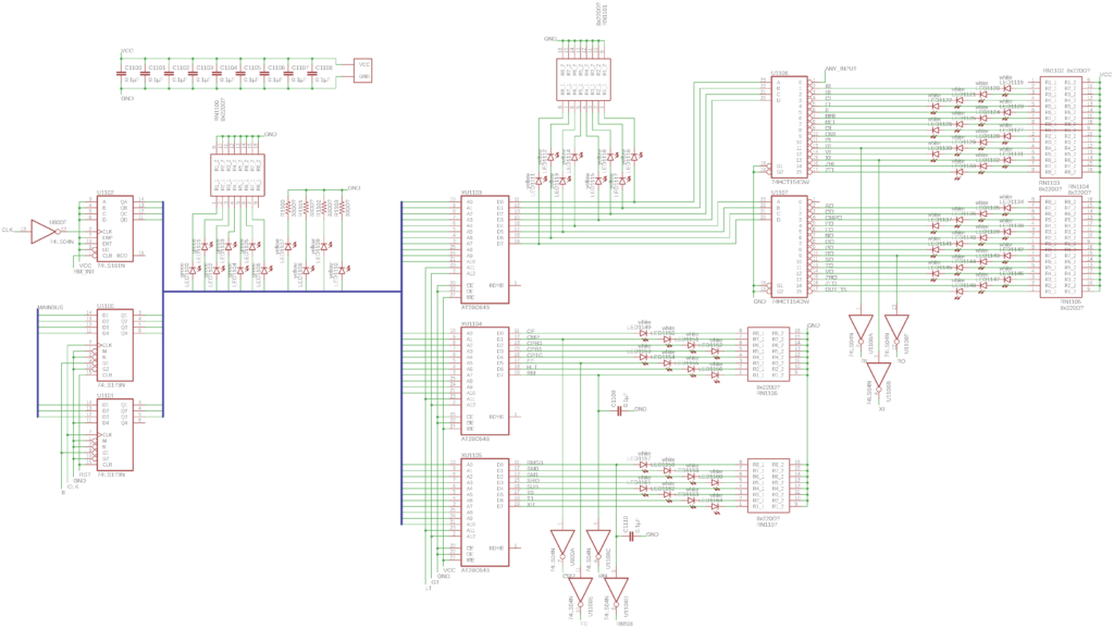
    Let’s start on the left side: There are two 4-bit register chips that store the current instruction code, which is 7 bits long. Above that, there’s a 4-bit counter that keeps track of the so-called microinstruction. Microinstructions are small steps that are exactly one clock cycle long and do a very basic task like moving a byte from one register to another. Multiple microinstructions are combined in sequence to execute an instruction which does something more complicated, like fetching a value from memory, or adding two numbers. Afterwards, a few extra microinstructions are executed to retrieve the next instruction from memory, this is called the “instruction fetch” cycle.

    There are some LED packs to display the instruction and microinstruction values. These two values are then fed into the next part of the circuit, which is combinational logic. Here it’s implemented using three ROM chips, similarly to the numerical output module (see part 4). This logic translates the instruction code and microinstruction step into the control signals that are fed to all other modules in the computer (input enables, output enables, other behaviour controls). The topmost chip’s outputs are fed into two 74HCT154 1-of-16 selectors (also called demultiplexers). This way, the 8 bits from the ROM output can be expanded out into 16 bus input enable controls and 16 bus output enable controls, using the fact that at most one input and one output need to be enabled at any point. All of these control signals are displayed using some white LEDs, and some of them are inverted, if the corresponding modules require a different signal polarity.

    To help the computer’s timing, the microinstruction counter increments on an inverted clock pulse (see the inverter on the left of the counter chip). This way, the computer alternates between executing a microinstruction (rising clock edge) and setting the control signals for the next microinstruction (falling clock edge).

    The details and implementation of instructions will be discussed in a separate post, but for now, let’s look at the PCB that I made from this schematic.

  • The 8 Bit Computer – Modules, Part 4

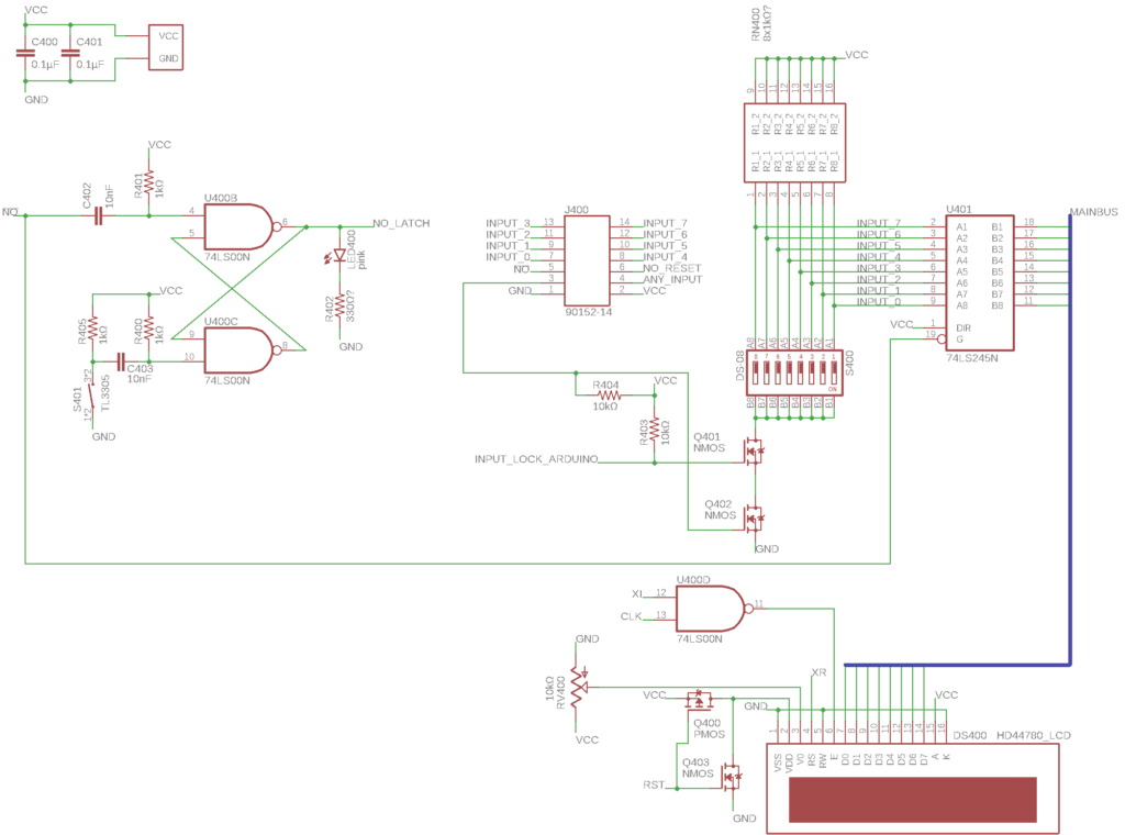
    User Input and LCD

    Schematic page 5: User Input & LCD

    These two modules are relatively simple additions that greatly improve the practical abilities of the computer. Let’s start with the LCD module (bottom).

    The main part of it is, of course, the LCD panel itself. I used a typical 16×2 character LCD display with a blue LED backlight. It has an HD44780 controller (or, more likely, a Chinese clone of it). That controller is ideal here, as it has an 8-bit parallel data interface that I can just directly connect to the main bus.

    The only things left to connect were contrast (potentiometer on the left), the enable signal (enabled when the LCD is selected and a clock pulse occurs), the register select pin (just another control line), and power/ground. The positive power supply is buffered through a CMOS inverter (two transistors) and is briefly turned off when the computer is reset. That is the easiest way to make sure that the LCD is cleared and reset whenever the computer resets.

    The user input module features the input switches themselves (S400, right), with pull-up resistors, and a bus transceiver for output. Alternatively, input can be supplied from the Arduino (see RAM module in part 2), or from an external connector (J400, middle of the page).

    To the left of the module, you can see the input enable latch (made of two NAND gates). It’s a simple SR-latch (set-reset-latch) that gets set when the user input is enabled (control signal NO). This lights a pink LED that signals that it’s waiting for input, and pauses the clock to give the user time to submit their input. The user then presses a button (S401) to reset the latch, resuming the clock and allowing the computer to read the input.

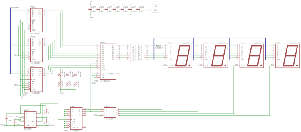
    Numerical Output

    Schematic page 9: Numerical Output

    This module also exists in Ben’s computer and is very similarly designed. It’s a simple seven-segment display that can show an 8-bit value in different representations.

    On the left side there are three 4-bit register chips. Two of them form an 8-bit register to store the value to be displayed, and the third one stores a 3-bit value that selects the display mode. Currently only modes 000 (decimal unsigned integer) and 001 (decimal signed integer) are implemented, but I could add things like hexadecimal or binary display options.

    On the bottom is a fast 555 timer connected to a 74LS161 4-bit binary counter. This is used to quickly switch between the four displays. What this means is that really only one of the four digits is being displayed at once, but it quickly switches between them so that it looks like all of them are lit constantly. This is also called “multiplexing”.

    In the middle, you can then see the last part of the display driver: The combinational logic. The inputs are the value to be displayed, the index of the currently lit digit, and the selected display mode. From that, you can determine which segments of the digit should be lit, which are the outputs of the combinational circuit. Instead of creating a circuit out of logic gates, it’s possible to use a ROM (read-only-memory) chip and store the correct outputs for each combination of inputs in the memory. Here, I used an AT28C64B ROM chip.

    Continued in Part 5.

  • The 8 Bit Computer – Modules, Part 3

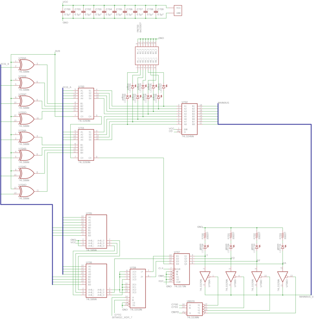
    The Arithmetic Unit and Comparator

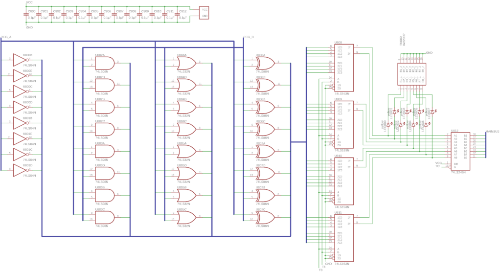
    Schematic page 7: ALU & Comparator

    Here we have two very important modules. The first one is the arithmetic unit, which can do addition and subtraction (top half of the page). Its main components are two 74LS283 4-bit adder chips (U700, U701) that are chained together to create an 8-bit adder. After the adder chips, there’s an LED pack to display the sum, and a bus transceiver to output the value to the rest of the computer.

    For subtraction, the module forms the two’s complement of B, effectively negating it, and then adds that to A. The two’s complement is formed by inverting every bit of B using the XOR gates on the left, and then adding 1 (done here using the carry input signal of the first adder chip). If you have no idea what any of that means, you should probably check out Ben’s videos on two’s complement and this module – the module is identical to his design.

    Something I never even thought of, before watching Ben’s series, is that an “add” instruction using this module doesn’t actually tell the computer to do the addition – the addition is always done and the sum is always available and can be seen on the LEDs. The only thing that an “add” instruction does is tell the computer to output that sum value onto the bus and store it in a register. Now that seems quite obvious and normal to me, but it blew my mind back then. There are many more things I learned about computers during this project that made me feel that way – which is why I consider this a very successful and valuable project for me.

    On the lower half of this page, you can see the comparator module. It allows the computer to compare two numbers by magnitude, which is quite important, as it opens the way to conditional branching – an essential concept in programming. It is implemented using two 74LS85 4-bit comparators (U705, U706) chained together, creating an 8-bit comparator. Next to that is a 74LS153 dual 4-to-1 selector (U709), which provides the selection logic that allows both signed and unsigned numbers to be correctly compared. Then there is a 4-bit register to store the states of the less than, equal, greater than and carry flags from both modules on this page, as well as some output logic that allows individual flag values to be output onto the main bus.

    Magnitude comparison of unsigned numbers is done quite simply: The comparator first checks the highest bits of the inputs and checks if they’re different. If they are, the input value that has a 1 in that place is definitely larger than the other input value – and so the corresponding output (A<B or A>B) is turned on. If the highest bits are the same, it checks the second highest bits the same way, then the third highest, and so on, until it finds a bit difference between the two inputs. If no difference is found after all bits have been checked, the numbers are equal, which is signalled using the A=B output.

    For signed numbers in two’s complement format, it seems a bit more complicated at first glance – but it turns out that the comparison can be done using the same 8-bit unsigned comparator, you just have to swap the A<B and A>B outputs if one input is negative and the other one isn’t. That is what the selector chip U709 does if a signed comparison is requested. If don’t see why that trick works, try it yourself (on paper)!

    The Bitwise Logic Module

    Schematic page 8: Bitwise Operations

    While this page is larger than the previous one, it’s actually a lot simpler. It implements bitwise NOT, AND, OR and XOR operations that can be applied to the registers A and B, which can be quite useful for programming and conditional logic.

    The components are straightforward: There are 8 logic gates of each kind named above, used to compute all four operations (NOT A, A AND B, A OR B, A XOR B). To the right there are four dual 4-to-1 selectors (74LS153, just like in the comparator above). They are used to select one of the four results that should be output to the bus. The selected value is then displayed on an LED pack and connected to a bus transceiver for output.

    This module, together with the arithmetic unit above, form the ALU (Arithmetic Logic Unit) of the computer, which does most of the useful work in most programs.

    Continued in Part 4.

  • The 8 Bit Computer – Modules, Part 2

    The Shift Register, Bus and Reset logic

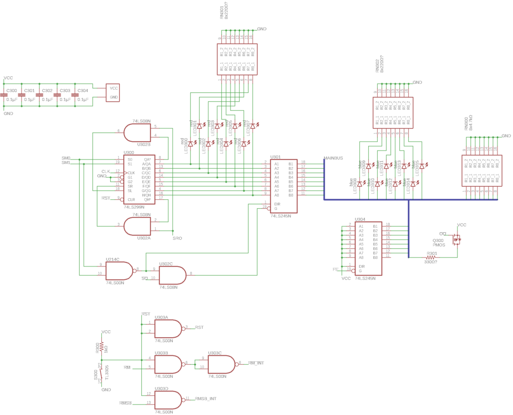
    Schematic page 3: Shift Register, Bus & Reset

    This page contains a few small independent modules. The largest one is the shift register, which occupies most of the left half of the page. A shift register can be used just like any other register, but it has an additional ability: it can shift the binary value inside it to the left or right. This can be quite useful in programming and calculations, as a shift to the left corresponds to a multiplication by 2 (and a right shift is a division by 2). I simply used a dedicated 8-bit shift register chip (74LS299, U300 on the left) to implement this.

    Usually, when shifting, the outermost bit that gets “shifted out” is simply discarded and the other side of the byte is filled with a zero. But sometimes, it can be useful to keep that bit and push it back into the other side of the byte instead. That operation is called a “roll”, and it is implemented using the two AND gates next to the chip. That way, the program can use the SRO (shift roll-over) control signal to enable this feature. In addition to the register chip, it also features a bus transceiver and LEDs as before, except that the bus transceiver is used bidirectionally here, both for reading and writing data to/from the shift register.

    The next part of this page, on the right side, contains some utilities for the main bus. There is an LED pack to show what is currently on the bus, as well as some pull-down resistors to hold the bus at all zeroes when no module is outputting data to it. Then there’s a bus transceiver and a transistor, which the control logic can use to set the bus to the values 01, FE or FF (hexadecimal) instead of the default 00. That is useful for the quick implementation of some instructions.

    Finally, this page houses the logic for the main reset signals of the computer (bottom left). The reset is triggered by the button S300. From that, the circuit produces reset signals in both polarities (active high and active low) that are distributed to all memory-containing modules, resetting the computer’s state (but not clearing the RAM). It also handles the two smaller reset signals RM and RMSB, which can be triggered either by the main reset or by the control logic.

    The RAM and Z register

    Schematic page 2: RAM & Z Register

    Now, we get to the largest page of the schematic. It contains the RAM (Random Access Memory), the memory address register, programming logic, and the general-purpose 16-bit register Z. The RAM module is relatively similar to Ben’s design, but expanded by a lot – from 16 bytes to 32KB.

    The RAM chip itself (HM62256) is the largest schematic symbol on the page (U200 in the middle right area). On its right side is the memory data bus which is used to transfer data (one byte at a time) to and from the memory. It’s connected to the main bus through a bus transceiver (directly to the right of the RAM chip). On the left side is the 15-bit-wide memory address bus, giving it a total of 32768 memory locations (=32KB of memory).

    The RAM module is relatively complex because there are two separate ways that the RAM needs to be accessed: by the computer, when running a program, and by the user/Arduino, when programming the computer (writing the program into memory). Both of these supply an address and data. Therefore, the module must select one of the given addresses (program address or externally supplied address) and the corresponding data lines, based on whether the computer is running or being programmed. This also happens in Ben’s design.

    The user must select between “run” mode and “programming” mode using the switch S200, which you can see at the bottom right of the page. Based on that signal, the address is selected, using 4 selector chips (74LS157) that you can see on the left of the main RAM chip.
    The address for “run” mode is stored in the 15-bit memory address register (top middle) which is made of four 4-bit register chips. The data in “run” mode is provided by the main bus, through the bus transceiver mentioned above.
    In “programming” mode, the address and data are provided either by manual switches (bottom middle), or by an Arduino, through some shift registers (74HCT595, bottom left).

    Now for the Z register. You can find it on the top left side of the page, and it’s not part of the RAM module. It’s on the same page because it is functionally related to the RAM, often serving as an address buffer for memory access. It consists of four 4-bit register chips and two 8-bit bus transceivers connected to the main bus.

    Last but not least, there are quite a few LED packs on this page: 16 LEDs showing the contents of the Z register, 15 LEDs showing the currently selected memory address (for “run” mode), and 8 LEDs showing the RAM contents at the currently selected memory address, as well as a green/red LED pair, indicating “run” or “programming” mode, respectively.

    Continued in Part 3.